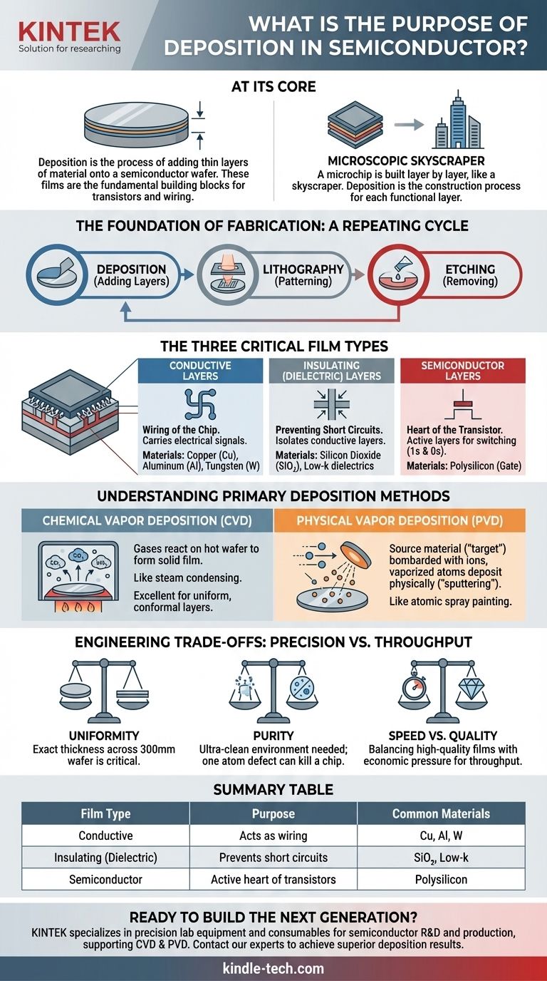
At its core, deposition is the process of adding thin layers of material onto a semiconductor wafer. These films, often just a few atoms thick, are the fundamental building blocks used to construct the intricate, three-dimensional structures that form transistors, capacitors, and the wiring that connects them. Without deposition, a silicon wafer would remain a blank slate, and the creation of an integrated circuit would be impossible.
A microchip is not carved from a single block; it is built up, layer by layer, like a microscopic skyscraper. Deposition is the fundamental construction process for adding each of these functional layers—be it conductive, insulating, or semiconducting.
The Foundation of Fabrication: Building Layer by Layer
Think of manufacturing a microchip not as sculpture (carving away material) but as a form of ultra-precise 3D printing. The process starts with a pristine, circular disc of silicon known as a wafer, which serves as the foundation.
The entire fabrication process involves a repeating cycle of adding layers (deposition), patterning them (lithography), and removing selected parts (etching). Deposition is the critical first step in this cycle, creating the raw material for each new level of the chip's architecture.
The Three Critical Film Types in a Semiconductor
Deposition isn't about adding just one type of material. Its purpose is to lay down different films with distinct electrical properties, each serving a specific role in the chip's function.
Conductive Layers: The Wiring of the Chip
These films act as the microscopic wires and interconnects that carry electrical signals between different components on the chip.
Materials like copper (Cu), aluminum (Al), and tungsten (W) are deposited to create the pathways for electricity to flow. Without these conductive layers, transistors would be isolated islands with no way to communicate.
Insulating (Dielectric) Layers: Preventing Short Circuits
These films are electrical insulators, meaning they do not conduct electricity. Their primary job is to isolate the conductive layers from each other.
Materials like silicon dioxide (SiO2) or more advanced low-k dielectrics are used. They prevent signals from "shorting out" or interfering with one another, which is critical as tens of billions of transistors are packed into a tiny area.
Semiconductor Layers: The Heart of the Transistor
These are the "active" layers that give a transistor its ability to switch on and off, representing the 1s and 0s of digital logic.
Depositing a material like polysilicon is essential for forming the gate of a transistor—the component that controls the flow of current. The precise properties of these deposited semiconductor films directly determine the chip's performance and power efficiency.
Understanding the Primary Deposition Methods
To achieve the required precision, engineers use two main families of deposition techniques, each with its own strengths.
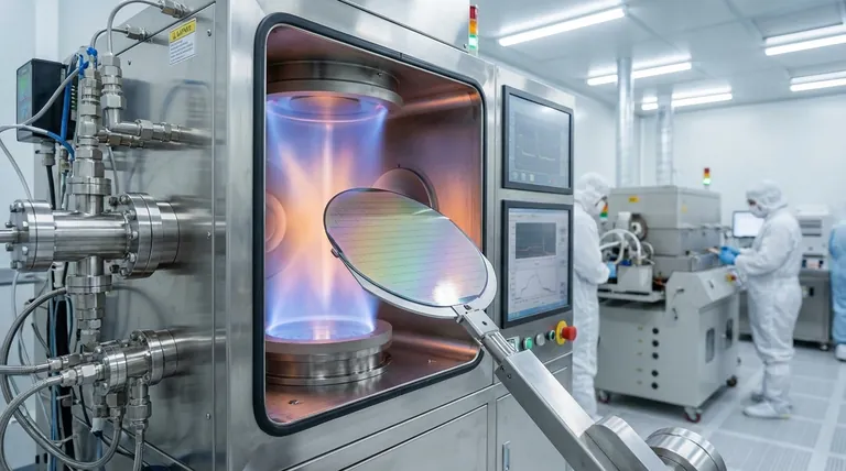
Chemical Vapor Deposition (CVD)
In CVD, the wafer is placed in a chamber and exposed to one or more reactive gases. These gases react on the hot wafer surface, leaving behind a solid film of the desired material as a byproduct.
Think of it like steam condensing on a cold window, but instead of water, a chemical reaction forms a solid, ultra-pure film. CVD is excellent for creating highly uniform and conformal layers that coat complex 3D structures evenly.
Physical Vapor Deposition (PVD)
In PVD, a source material (a "target") is bombarded with high-energy ions, which knocks atoms loose from the target. These vaporized atoms then travel through a vacuum and physically deposit onto the wafer's surface, like a form of atomic spray painting.
This method, often called sputtering, is highly effective for depositing metals and other materials in a direct line-of-sight fashion.
The Trade-offs: Precision vs. Throughput
The purpose of deposition is to create perfect films, but achieving this goal involves navigating critical engineering trade-offs.
The Challenge of Uniformity
The deposited film must have the exact same thickness across the entire 300mm wafer. A variation of even a few atoms from one side to the other can cause billions of transistors to perform differently, leading to a failed chip.
The Problem of Purity
The deposited films must be exceptionally pure. A single unwanted foreign atom in a critical layer can alter its electrical properties and create a defect that kills the entire chip. This requires an ultra-clean vacuum environment.
The Speed vs. Quality Dilemma
Manufacturing is a business, and throughput (wafers per hour) is critical for cost. Generally, depositing a film faster can reduce its quality, uniformity, or purity. Engineers must constantly balance the need for high-quality films with the economic pressure to produce chips quickly.
How to Apply This to Your Goal
The importance of deposition depends on your specific focus within the semiconductor industry.
- If your primary focus is device performance: The quality of deposited dielectric films (like the gate insulator) directly dictates transistor speed and power leakage.
- If your primary focus is manufacturing yield: The uniformity and defect-free nature of deposited layers are the most critical factors in producing a high number of working chips per wafer.
- If your primary focus is advanced architecture: New deposition techniques like Atomic Layer Deposition (ALD) are what enable the move to complex 3D transistor structures like FinFETs and Gate-All-Around (GAA).
Ultimately, understanding deposition is understanding the fundamental language used to construct every modern microchip.
Summary Table:
| Film Type | Purpose | Common Materials |
|---|---|---|
| Conductive | Acts as wiring for electrical signals | Copper (Cu), Aluminum (Al), Tungsten (W) |
| Insulating (Dielectric) | Prevents short circuits between conductive layers | Silicon Dioxide (SiO₂), Low-k dielectrics |
| Semiconductor | Forms the active heart of transistors | Polysilicon |
Ready to build the next generation of microchips? The quality of your deposited films directly determines device performance and manufacturing yield. KINTEK specializes in precision lab equipment and consumables for semiconductor R&D and production. Whether you are developing advanced architectures or optimizing for high yield, our solutions support critical processes like CVD and PVD. Contact our experts today to discuss how we can help you achieve superior deposition results.
Visual Guide
Related Products
- RF PECVD System Radio Frequency Plasma-Enhanced Chemical Vapor Deposition RF PECVD
- Evaporation Boat for Organic Matter
- Thin-Layer Spectral Electrolysis Electrochemical Cell
- Side Window Optical Electrolytic Electrochemical Cell
- Reference Electrode Calomel Silver Chloride Mercury Sulfate for Laboratory Use
People Also Ask
- How does Radio Frequency Enhanced Plasma Chemical Vapour Deposition (RF-PECVD) work? Learn the Core Principles
- How does plasma enhance CVD? Unlock Low-Temperature, High-Quality Film Deposition
- What is plasma enhanced chemical vapour deposition process? Unlock Low-Temperature, High-Quality Thin Films
- What is plasma enhanced chemical Vapour deposition process used for fabrication of? A Guide to Low-Temperature Thin Films
- What is plasma chemical vapor deposition? A Low-Temperature Thin Film Coating Solution


