The low-temperature annealing process acts as a critical stabilization step that transforms a liquid colloid into a functional solid layer. By heating the substrate to typically 150°C for 30 minutes, the process rapidly evaporates the ethanol solvent to create a dense, stable thin film of Nickel Oxide nanoparticles on the Indium Tin Oxide (ITO) surface.
The ultimate goal of this thermal treatment is to physically restructure the nanoparticle layer, strengthening electronic pathways and reducing defects to ensure efficient charge migration within the device.
Mechanisms of Structural Formation
Rapid Solvent Removal
The immediate function of annealing is the removal of the carrier medium. Heating the device drives off the ethanol solvent used in the Nickel Oxide colloid.
This evaporation occurs rapidly, preventing the liquid from interfering with the final film structure.
Creating a Dense Film
Once the solvent is removed, the remaining Nickel Oxide nanoparticles must settle into a cohesive structure.
The annealing process promotes the formation of a dense and stable thin film, ensuring uniform coverage across the ITO substrate.
Optimization of Electrical Properties
Strengthening Transmission Channels
For a device to function correctly, electrons must move freely between nanoparticles.
Annealing strengthens the electronic transmission channels between individual particles, effectively bridging the gaps that exist in the liquid colloid state.
Minimizing Transport Barriers
Imperfections in a film can act as traps for electrical charges, reducing efficiency.
This thermal process actively reduces physical defects within the nanoparticle layer, removing obstacles that would otherwise hinder performance.
Understanding Process Constraints
Specificity of Conditions
The effectiveness of this process relies on adherence to specific parameters, typically 150°C for 30 minutes.
These conditions are calibrated to provide enough energy for solvent evaporation and particle settling without necessitating high-temperature sintering.
The Consequence of Defects
The reduction of defects is not merely cosmetic; it is fundamental to the device's operation.
Without this specific annealing step, the charge migration essential for the device's function would be inefficient or erratic due to structural interruptions.
Making the Right Choice for Your Goal
- If your primary focus is Structural Integrity: Ensure the full 30-minute duration is met to allow complete solvent evaporation and the formation of a dense, stable film.
- If your primary focus is Electrical Efficiency: Prioritize precise temperature control at 150°C to maximize the strengthening of electronic transmission channels and minimize defects.
Success in this fabrication step relies on balancing rapid solvent removal with the time required to forge strong inter-particle connections.
Summary Table:
| Feature | Description | Key Benefit |
|---|---|---|
| Temperature | 150°C for 30 Minutes | Rapid solvent evaporation without sintering |
| Carrier Removal | Ethanol Solvent Elimination | Prevents liquid interference in film structure |
| Film Density | Nanoparticle Consolidation | Ensures uniform coverage on ITO substrates |
| Connectivity | Strengthened Electronic Channels | Enhances charge migration and device efficiency |
| Quality Control | Physical Defect Reduction | Minimizes transport barriers and charge traps |
Elevate Your Material Research with KINTEK
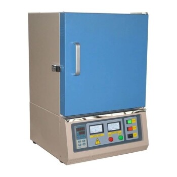
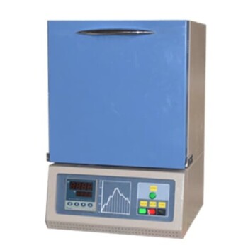
Precision in thin-film fabrication requires the right thermal and processing tools. KINTEK specializes in high-performance laboratory equipment, including high-temperature furnaces (muffle, vacuum, CVD) and high-pressure reactors designed to meet the rigorous demands of battery research and electronics development.
Whether you are refining Nickel Oxide layers or developing advanced electrolytic cells, our comprehensive range of crushing, milling, and heating solutions ensures your substrates achieve maximum electrical efficiency. Contact KINTEK today to discover how our high-precision equipment and quality consumables like ceramics and crucibles can optimize your lab's performance!
References
- Amani Kamil, Shvan H Mohammed. Photochemical synthesized NiO nanoparticles based dye-sensitized solar cells: a comparative study on the counter lectrodes and dye-sensitized concentrations. DOI: 10.15251/jor.2021.173.299
This article is also based on technical information from Kintek Solution Knowledge Base .
Related Products
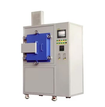
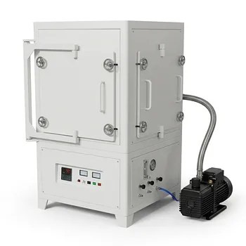
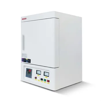
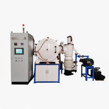
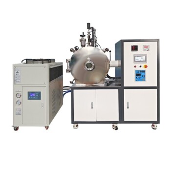
- Vacuum Heat Treat Furnace with Ceramic Fiber Liner
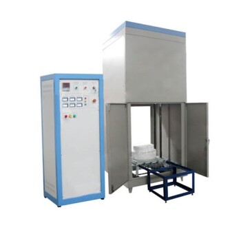
- Controlled Nitrogen Inert Hydrogen Atmosphere Furnace
- 1700℃ Controlled Atmosphere Furnace Nitrogen Inert Atmosphere Furnace
- 1200℃ Controlled Atmosphere Furnace Nitrogen Inert Atmosphere Furnace
- 1400℃ Controlled Atmosphere Furnace with Nitrogen and Inert Atmosphere
People Also Ask
- What are the disadvantages of vacuum heat treatment? High Costs and Technical Limitations Explained
- What is the principle of vacuum heat treatment? Achieve Superior Material Properties with Total Control
- What are the three primary cooling methods for a vacuum heat treatment furnace? Optimize Hardness & Surface Finish
- What are the failures related to heat treating operations? Prevent Distortion, Cracking & Soft Spots
- How does a vacuum heat treatment work? Achieve Superior Material Properties in a Pristine Environment