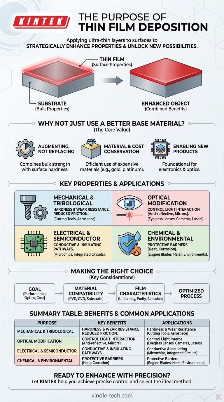
The fundamental purpose of thin film deposition is to apply an ultra-thin layer of a specific material onto the surface of another object, known as a substrate. This process is used to intentionally alter the surface properties of the substrate, giving it new characteristics—such as wear resistance, electrical conductivity, or anti-reflection—that it does not inherently possess.
Thin film deposition is not about creating a new material from scratch, but about strategically enhancing an existing one. It allows engineers to combine the bulk properties of a substrate (like strength or low cost) with the specialized surface properties of a different material (like hardness or optical transparency), solving problems that a single material cannot.
Why Not Just Use a Better Base Material?
The core value of thin film deposition lies in its efficiency and precision. It separates the structural requirements of an object from its surface requirements, which is a powerful engineering advantage.
Augmenting, Not Replacing
Most components are chosen for their bulk properties, such as the strength of steel, the light weight of aluminum, or the low cost of plastic.
Thin film deposition adds critical surface properties that these base materials lack. For example, a hard, low-friction coating can be applied to a steel tool bit, combining the tool's toughness with a superior cutting surface.
Material and Cost Conservation
Many high-performance materials like gold, platinum, or diamond-like carbon are rare and expensive.
Deposition techniques allow an infinitesimally thin, and therefore cost-effective, layer of this precious material to be applied to a cheaper substrate, providing the desired benefit without the prohibitive cost of making the entire object from it.
Enabling Entirely New Products
This technology is foundational to modern electronics and optics. A silicon wafer is just a piece of silicon until thin film deposition is used to build up the intricate layers of conductive and insulating materials that form a microchip.
Key Properties Achieved Through Deposition
The specific goal of deposition can vary dramatically, but it generally falls into a few key categories of surface modification.
Mechanical and Tribological Enhancement
One of the most common uses is to improve a surface's mechanical behavior.
This includes increasing hardness and wear resistance for cutting tools or aerospace components, and reducing the coefficient of friction for moving parts in engines.
Optical Modification
In optics, deposition is used to precisely control how light interacts with a surface.
This can involve creating anti-reflective coatings for eyeglass lenses and camera optics or making highly reflective mirrors for telescopes and lasers.
Electrical and Semiconductor Applications
Thin film deposition is the cornerstone of the semiconductor industry.
It is used to grow the highly pure electronic materials and create the conductive or insulating pathways that form transistors and integrated circuits on a silicon substrate.
Chemical and Environmental Barriers
Thin films can serve as a protective shield for the underlying substrate.
These barrier coatings can protect aerospace engine blades from extreme heat and prevent metal parts from corroding in harsh chemical environments.
Understanding the Key Considerations
The choice of a deposition technique is not a one-size-fits-all decision. It is a calculated trade-off based on the final goal, the materials involved, and the required characteristics of the film.
The Central Question: What is Your Goal?
The desired outcome dictates the process. A coating for a decorative plastic part has vastly different requirements than a thermal barrier for a jet engine turbine blade.
Material Compatibility
The chosen technique, such as Physical Vapor Deposition (PVD) or Chemical Vapor Deposition (CVD), must be compatible with both the substrate material and the material being deposited. Some processes require high temperatures that certain substrates cannot tolerate.
Required Film Characteristics
Different methods produce films with different properties. Factors like the required uniformity across the surface, chemical purity, physical density, and how well the film adheres to the substrate are critical in selecting the right process.
Making the Right Choice for Your Goal
To apply this knowledge effectively, align your primary objective with the capabilities of the deposition process.
- If your primary focus is performance and durability: Select a process that creates a dense, highly adherent film to maximize wear, corrosion, or thermal resistance.
- If your primary focus is optical or electronic properties: The key is choosing a method that guarantees high purity and precise control over film thickness and uniformity.
- If your primary focus is cost-effectiveness and material savings: The goal is to use a minimal amount of a valuable coating material efficiently on a low-cost substrate.
Ultimately, thin film deposition is a precise engineering tool that grants you control over the very surface of an object, unlocking a new level of performance and possibility.
Summary Table:
| Purpose of Thin Film Deposition | Key Benefits | Common Applications |
|---|---|---|
| Mechanical/Tribological Enhancement | Increases hardness, wear resistance, and reduces friction. | Cutting tools, aerospace components, engine parts. |
| Optical Modification | Controls light interaction (anti-reflective, highly reflective). | Eyeglass lenses, camera optics, telescopes, lasers. |
| Electrical/Semiconductor Applications | Creates conductive/insulating pathways for electronics. | Microchips, transistors, integrated circuits. |
| Chemical/Environmental Barriers | Protects substrates from heat, corrosion, and harsh environments. | Aerospace engine blades, metal parts in corrosive settings. |
Ready to enhance your materials with precision thin film deposition?
At KINTEK, we specialize in providing advanced lab equipment and consumables for all your thin film deposition needs. Whether you're developing cutting-edge semiconductors, durable protective coatings, or high-performance optical components, our solutions deliver the accuracy, reliability, and material compatibility required for superior results.
Let KINTEK help you:
- Achieve precise control over film thickness, uniformity, and adhesion.
- Select the ideal deposition method (PVD, CVD, etc.) for your specific substrate and performance goals.
- Optimize your process for cost-effectiveness and material efficiency.
Unlock the full potential of your materials—contact our experts today for a personalized consultation!
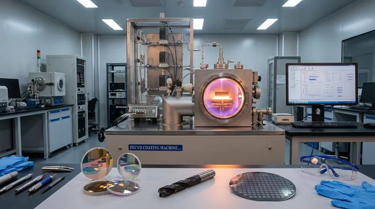
Visual Guide
Related Products
- Aluminized Ceramic Evaporation Boat for Thin Film Deposition
- Tungsten Evaporation Boat for Thin Film Deposition
- Electron Beam Evaporation Coating Oxygen-Free Copper Crucible and Evaporation Boat
- Molybdenum Tungsten Tantalum Evaporation Boat for High Temperature Applications
- HFCVD Machine System Equipment for Drawing Die Nano-Diamond Coating
People Also Ask
- What are the applications of thin films deposition? Unlock New Possibilities for Your Materials
- What is the widely used boat made of in thermal evaporation? Choosing the Right Material for High-Purity Deposition
- What is the chemical method for thin film deposition? Build Films from the Molecular Level Up
- Why is an alumina boat and Ti3AlC2 powder bed necessary for Ti2AlC sintering? Protect MAX Phase Purity
- What are thin films deposited by evaporation? A Guide to High-Purity Coating


