In the context of Scanning Electron Microscopy (SEM), sputtering is a critical sample preparation technique. It is a coating process used to deposit an ultrathin layer of electrically conductive material, such as gold or platinum, onto a non-conductive or poorly conductive sample. This coating prevents the buildup of electrical charge on the sample's surface during SEM analysis, which is essential for acquiring a clear, stable, and accurate image.
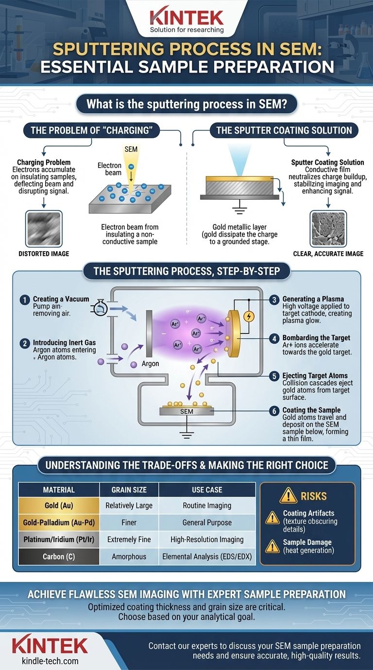
The core problem sputtering solves for SEM is "charging"—the accumulation of electrons on an insulating sample from the SEM's electron beam. By making the sample's surface conductive, sputtering dissipates this charge, eliminating image distortion and revealing the true surface topography.
Why Sputtering is Essential for SEM
The Problem of "Charging"
A Scanning Electron Microscope works by bombarding a sample with a focused beam of high-energy electrons.
When these electrons strike a conductive material, the excess charge is conducted away to the ground. On an insulating material, like a polymer, ceramic, or most biological specimens, the electrons have nowhere to go and accumulate on the surface.
How Charging Distorts Images
This trapped negative charge severely disrupts the imaging process. It can deflect the incoming electron beam and alter the emission of the signal electrons used to form the image.
The result is a distorted and unusable image, often characterized by overly bright patches, streaks, shifting, and a complete loss of fine surface detail.
The Sputter Coating Solution
Sputter coating, also known as sputter deposition, solves this problem by rendering the sample's surface conductive.
The thin metallic film provides a path for the incident electrons to travel to the grounded SEM sample stage. This neutralizes the charge buildup, stabilizes the imaging process, and often enhances the signal-to-noise ratio by improving the emission of secondary electrons.
The Sputtering Process, Step-by-Step
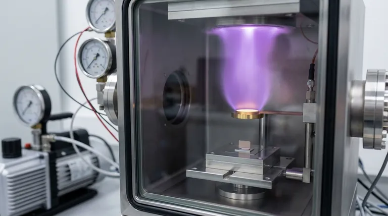
The technique is a physical vapor deposition (PVD) process that occurs inside a dedicated piece of equipment called a sputter coater.
1. Creating a Vacuum
First, the SEM sample (the substrate) and a small disc of the coating material (the target, e.g., gold) are placed inside a sealed vacuum chamber. The air is pumped out to create a low-pressure environment, which prevents gas molecules from interfering with the process.
2. Introducing an Inert Gas
A small, controlled amount of an inert gas—almost always Argon (Ar)—is then introduced into the chamber.
3. Generating a Plasma
A strong electric field is applied within the chamber, typically by applying a high negative voltage to the target, making it the cathode. This high voltage ionizes the argon gas atoms, stripping them of electrons.
This process creates a distinctive glow and fills the chamber with a mixture of positively charged argon ions (Ar+) and free electrons, which is known as a plasma.
4. Bombarding the Target
The positively charged argon ions are powerfully accelerated by the electric field and slam into the negatively charged target material.
5. Ejecting Target Atoms
This high-energy bombardment is a purely physical process. The momentum from the argon ions is transferred to the atoms in the target, setting off "collision cascades" within the material.
When these cascades reach the surface, they have enough energy to knock individual atoms of the target material completely free. This ejection of atoms is the "sputtering" phenomenon.
6. Coating the Sample
The ejected target atoms (e.g., gold atoms) travel in straight lines through the vacuum and land on all exposed surfaces of the SEM sample below.
These atoms slowly build up on the sample, forming an ultrathin, uniform conductive film, typically only a few to tens of nanometers thick.
Understanding the Trade-offs
While essential, the sputter coating process is not without considerations that require an expert's judgment.
Choosing the Right Coating Material
The material you choose to sputter has a direct impact on image quality.
- Gold (Au) is a common, cost-effective choice that provides a strong signal but has a relatively large grain size, which can obscure very fine nanoscale features.
- Gold-Palladium (Au-Pd) offers a finer grain size than pure gold and is a good general-purpose compromise.
- Platinum (Pt) or Iridium (Ir) produce extremely fine-grained coatings and are the preferred choice for very high-magnification, high-resolution imaging.
- Carbon (C) is used when performing elemental analysis (EDS/EDX), as its low atomic number does not interfere with the X-ray signals from the elements of interest in the sample.
Risk of Coating Artifacts
The coating itself has a texture. If the coating is too thick or has a large grain size, you may end up imaging the structure of the coating rather than the true surface of your sample.
Potential for Sample Damage
The sputtering process generates a small amount of heat. While minimal, this can be enough to damage extremely delicate or heat-sensitive samples, such as certain biological tissues.
Making the Right Choice for Your Goal
Selecting the correct coating strategy is fundamental to good SEM analysis. Your choice should be dictated by your ultimate analytical goal.
- If your primary focus is routine imaging of robust samples: A standard gold (Au) coating is efficient, cost-effective, and provides an excellent signal for most applications.
- If your primary focus is high-resolution imaging of fine surface details: Use a finer-grained material like platinum (Pt) or iridium (Ir) to ensure the coating does not obscure the features you wish to see.
- If your primary focus is elemental analysis (EDS/EDX): You must use a carbon coater to deposit a carbon film, which avoids introducing metallic X-ray peaks that would contaminate your spectrum.
Ultimately, understanding the sputtering process empowers you to prepare samples correctly, ensuring the SEM data you collect is both accurate and reliable.
Summary Table:
| Aspect | Key Consideration |
|---|---|
| Primary Goal | Prevent sample charging during SEM analysis for stable, clear imaging. |
| Coating Materials | Gold (routine), Platinum/Iridium (high-res), Carbon (elemental analysis). |
| Process Type | Physical Vapor Deposition (PVD) in a vacuum chamber. |
| Critical Factor | Coating thickness and grain size must be optimized to avoid obscuring sample details. |
Achieve Flawless SEM Imaging with Expert Sample Preparation
Are you struggling with charging artifacts or unclear images in your SEM analysis? The right sputter coating is critical for success. KINTEK specializes in lab equipment and consumables, providing reliable sputter coaters and expert guidance to help you select the ideal coating material and parameters for your specific samples—whether they are polymers, ceramics, or biological specimens.
Let us help you enhance your lab's capabilities. Contact our experts today to discuss your SEM sample preparation needs and ensure accurate, high-quality results.
Visual Guide
Related Products
- Infrared Transmission Coating Sapphire Sheet Substrate Window
- Electron Beam Evaporation Coating Oxygen-Free Copper Crucible and Evaporation Boat
- 400-700nm Wavelength Anti Reflective AR Coating Glass
- Custom CVD Diamond Coating for Lab Applications
- Molybdenum Tungsten Tantalum Special Shape Evaporation Boat
People Also Ask
- What is the optical coating? Master Light Control for Superior Optical Performance
- What is optical coating used for? Control Light for Enhanced Performance in Your Applications
- What are the applications of optical coating? Unlock Advanced Light Control for Your Industry
- What is the thinnest coating? Unlocking Unique Properties at the Atomic Scale
- Is Sputter Tint good? Premium Heat Rejection & Long-Term Durability Explained


