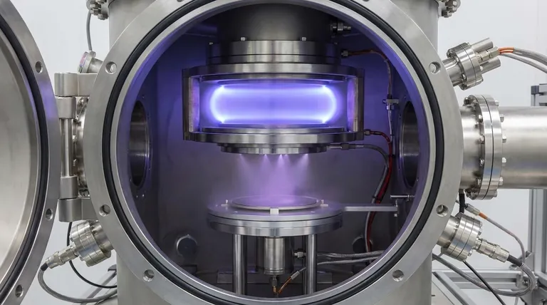
In essence, magnetron sputtering is a highly controlled physical vapor deposition (PVD) technique used to create thin films. The process takes place in a vacuum and involves bombarding a target material with high-energy ions from a plasma. These ions physically knock off, or "sputter," atoms from the target, which then travel and deposit onto a substrate, forming a uniform coating. The "magnetron" part is crucial, as it uses a magnetic field to trap electrons near the target, dramatically increasing the efficiency of the ion creation process.
The central takeaway is that magnetron sputtering isn't just about bombarding a target; it's about using a clever magnetic trap. This trap creates a dense, localized plasma that makes the sputtering process faster, more stable, and allows it to operate at lower pressures than other methods.
The Core Mechanism: From Gas to Solid Film
To understand magnetron sputtering, it's best to break it down into a sequence of events. Each step builds upon the last, culminating in the creation of a high-quality thin film.
Step 1: Creating the Vacuum Environment
The entire process must occur in a vacuum chamber. This removes air and other particles that could contaminate the film or interfere with the sputtering process.
Step 2: Introducing an Inert Gas
A continuous flow of an inert gas, almost always argon (Ar), is introduced into the chamber. This gas is not part of the final film; it serves only to create the ions needed for bombardment.
Step 3: Igniting the Plasma
A high DC voltage (often -300V or more) is applied to the target material, which acts as the cathode (negative electrode). The substrate holder or chamber walls act as the anode (positive electrode). This high voltage energizes the argon gas, stripping electrons from the argon atoms and creating a glowing plasma of free electrons and positively charged argon ions (Ar+).
Step 4: The Critical Role of the Magnetic Field
This is the key to magnetron sputtering. Magnets placed behind the target create a magnetic field that is perpendicular to the electric field. This field traps the free electrons, forcing them into a long, spiral path directly in front of the target.
By trapping electrons, the magnetic field dramatically increases the probability that they will collide with and ionize more argon atoms. This creates a much denser, more intense plasma right where it's needed most—at the target's surface.
Step 5: Ion Bombardment and Atom Ejection
The negatively charged target powerfully attracts the positively charged argon ions from the dense plasma. These ions accelerate and collide with the target surface at high speed.
This collision transfers significant energy to the atoms in the target. If the energy transferred is greater than the material's binding energy, target atoms are physically ejected, or sputtered, into the vacuum chamber.
Step 6: Deposition onto the Substrate
The ejected target atoms are neutral and travel in a straight line from the target. They eventually strike the substrate (the part being coated) and condense on its surface, gradually building up a thin, uniform film.
Understanding the Trade-offs and Considerations
While powerful, magnetron sputtering is not a universal solution. Understanding its inherent characteristics is crucial for proper application.
Line-of-Sight Deposition
Sputtered atoms travel in straight lines. This means the process is highly directional, which can make it challenging to evenly coat complex, three-dimensional shapes without sophisticated substrate rotation.
Target Material Limitations
Standard DC magnetron sputtering works exceptionally well for electrically conductive materials. However, if the target is an insulating (dielectric) material, the positive ion bombardment will cause a positive charge to build up on its surface, eventually repelling the ions and stopping the process. Coating insulators requires more complex techniques like RF (Radio Frequency) sputtering.
Process Complexity
This is not a simple benchtop procedure. It requires significant capital equipment, including vacuum chambers, high-voltage power supplies, cooling systems, and gas flow controllers. The process parameters must be meticulously controlled to achieve repeatable results.
Making the Right Choice for Your Goal
Magnetron sputtering is chosen for specific outcomes. Your end goal dictates whether it is the most suitable technique for your application.
- If your primary focus is high-quality, dense films: Magnetron sputtering excels at creating films with excellent adhesion, controlled stoichiometry, and high density.
- If your primary focus is coating with complex alloys: The process faithfully transfers the composition from the target to the substrate, making it ideal for depositing alloys without altering their makeup.
- If you are coating a heat-sensitive substrate: The process generates less radiant heat compared to thermal evaporation, making it a superior choice for coating plastics or other temperature-sensitive materials.
- If your primary focus is deposition rate and control: The magnetic confinement creates a highly efficient process, offering excellent control over film thickness and faster deposition rates than non-magnetron sputtering.
Ultimately, magnetron sputtering is a precise and versatile tool for engineering surfaces at the atomic level.
Summary Table:
| Key Aspect | Description |
|---|---|
| Process Type | Physical Vapor Deposition (PVD) |
| Core Mechanism | Ion bombardment of a target material in a vacuum, enhanced by a magnetic field |
| Primary Gas Used | Argon (Ar) |
| Key Advantage | High deposition rates, excellent film density and adhesion, operates at lower pressures |
| Ideal For | Conductive materials, alloys, heat-sensitive substrates |
| Limitation | Line-of-sight deposition; insulating targets require RF sputtering |
Ready to achieve precise, high-quality thin films for your laboratory?
At KINTEK, we specialize in providing advanced lab equipment, including magnetron sputtering systems, to meet your specific research and production needs. Whether you're working with conductive materials, complex alloys, or temperature-sensitive substrates, our solutions deliver superior film density, adhesion, and controlled stoichiometry.
Contact us today to discuss how our expertise and reliable equipment can enhance your coating processes and drive your innovations forward.
Visual Guide

Related Products
- Spark Plasma Sintering Furnace SPS Furnace
- RF PECVD System Radio Frequency Plasma-Enhanced Chemical Vapor Deposition RF PECVD
People Also Ask
- What is the difference between spark plasma sintering and flash sintering? A Guide to Advanced Sintering Methods
- What are the fundamentals of spark plasma sintering process? Unlock Rapid, High-Performance Material Consolidation
- What is SPS sintering method? A Guide to High-Speed, High-Performance Material Fabrication
- What technical advantages does a Spark Plasma Sintering (SPS) furnace offer for LZP ceramics? Enhance Ionic Conductivity
- Why are Spark Plasma Sintering (SPS) furnaces or hot presses utilized in the preparation of Li3PS4 solid electrolytes?

