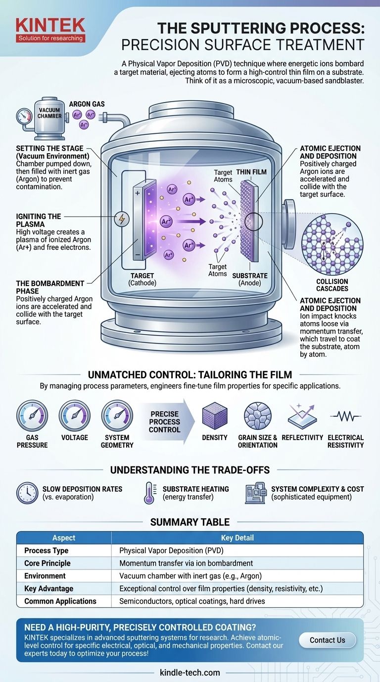
In essence, sputtering is a vacuum deposition process where atoms are physically ejected from a solid material, called the "target," and deposited as a thin, highly controlled film onto a surface, known as the "substrate." It functions like a microscopic sandblaster, using energetic ions of a gas instead of sand to dislodge particles from the source material, which then coat the desired object.
The core principle of sputtering is momentum transfer. It is not a chemical reaction but a physical process where high-energy ions bombard a target material in a vacuum, knocking atoms loose which then travel and build a precise, uniform film on a substrate.
The Core Mechanism: From Plasma to Film
To understand sputtering, it's best to break it down into the sequence of events that occur within the vacuum chamber. Each step is critical for achieving the final, high-quality coating.
Setting the Stage: The Vacuum Environment
The entire process must take place in a vacuum chamber. This chamber is pumped down to a very low pressure and then backfilled with a small, controlled amount of an inert gas, most commonly Argon.
The vacuum is crucial because it ensures the sputtered atoms can travel from the target to the substrate without colliding with unwanted air molecules, which would contaminate the film.
Igniting the Plasma
A high voltage is applied within the chamber, making the source material (the target) a negative electrode (cathode) and the object to be coated (the substrate) an anode.
This strong electric field energizes the Argon gas, stripping electrons from the Argon atoms. This creates a glowing, ionized gas known as a plasma, which is a mixture of positively charged Argon ions (Ar+) and free electrons.
The Bombardment Phase
The positively charged Argon ions are now powerfully attracted and accelerated toward the negatively charged target.
They collide with the surface of the target with significant kinetic energy. This is the central action of the sputtering process.
Atomic Ejection and Deposition
This high-energy ion bombardment sets off a series of "collision cascades" within the target material, similar to a billiard break on an atomic scale.
When these cascades reach the surface, atoms of the target material are physically knocked loose, or "sputtered," into the chamber. These ejected atoms travel through the vacuum and land on the substrate, gradually building up a thin film atom by atom.
Why Sputtering Offers Unmatched Control
The reason sputtering is so widely used in high-technology applications is the exceptional level of control it provides over the final film's properties. This isn't an accident; it's a direct result of the physics involved.
The Physics of Precision
The efficiency and outcome of the process are determined by several key factors, including the energy of the bombarding ions, the masses of the gas ions and target atoms, and the surface binding energy of the target material itself.
By precisely managing the gas pressure, voltage, and system geometry, engineers can fine-tune the sputtering process to achieve a desired deposition rate and film quality.
Tailoring the Final Film
This level of control allows for the creation of films with highly specific and repeatable characteristics.
Engineers can precisely dictate a film's density, grain size, grain orientation, reflectivity, and electrical resistivity. This is critical for manufacturing items like semiconductor wafers, optical lenses, and hard drives.
Understanding the Trade-offs
While powerful, sputtering is not the perfect solution for every scenario. Acknowledging its limitations is key to using it effectively.
Potentially Slow Deposition Rates
Compared to some other methods like thermal evaporation, sputtering can be a slower process. This can impact throughput in high-volume manufacturing environments.
Substrate Heating
The constant bombardment of energetic particles (including ions and electrons) can transfer a significant amount of energy to the substrate, causing it to heat up. This can be a problem for heat-sensitive substrates like certain plastics.
System Complexity and Cost
Sputtering systems are sophisticated pieces of equipment. They require robust vacuum chambers, high-voltage DC or RF power supplies, and precise gas flow controllers, making the initial investment higher than for simpler coating techniques.
Making the Right Choice for Your Goal
Selecting a surface treatment process depends entirely on the desired outcome. Sputtering is the superior choice for applications demanding precision and purity.
- If your primary focus is high-purity, dense films: Sputtering is ideal because it physically transfers material without melting it, perfectly preserving the source material's composition.
- If your primary focus is coating with complex alloys or compounds: Sputtering excels at maintaining the original material's stoichiometry (elemental ratio) in the final film.
- If your primary focus is creating films with specific electrical or optical properties: The fine control over the film's atomic structure makes sputtering the definitive choice for advanced electronic and optical components.
Ultimately, sputtering empowers the creation of advanced materials by providing atomic-level control over the coating process.
Summary Table:
| Aspect | Key Detail |
|---|---|
| Process Type | Physical Vapor Deposition (PVD) |
| Core Principle | Momentum transfer via ion bombardment |
| Environment | Vacuum chamber with inert gas (e.g., Argon) |
| Key Advantage | Exceptional control over film properties (density, resistivity, etc.) |
| Common Applications | Semiconductors, optical coatings, hard drives |
Need a high-purity, precisely controlled coating for your laboratory materials?
At KINTEK, we specialize in advanced lab equipment, including sputtering systems designed for research and development. Our solutions help you achieve the atomic-level control necessary for creating thin films with specific electrical, optical, and mechanical properties.
Whether you are working with semiconductors, optics, or novel materials, our expertise can help you optimize your process. Contact our experts today to discuss your specific surface treatment requirements and discover how KINTEK's lab equipment can enhance your results.
Visual Guide