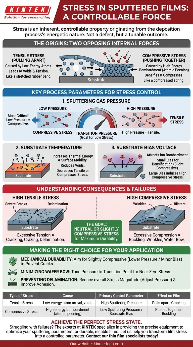
Stress is an inherent property of sputtered thin films, originating directly from the energetic nature of the deposition process. Films can exhibit either tensile stress, where the film is being pulled apart, or compressive stress, where it is being pushed together. The type and magnitude of this stress are not defects but are controllable outcomes determined by the specific parameters used during the sputtering deposition.
The stress within a sputtered film is the single most important factor determining its mechanical stability. Understanding that this stress is a direct, tunable result of process parameters—primarily sputtering pressure—is the key to preventing common failures like cracking, buckling, and delamination.
The Origins of Film Stress: A Tale of Two Forces
Fundamentally, film stress arises from the arrangement of atoms as they land and form the film. The energy they possess upon arrival dictates this arrangement, creating one of two opposing internal forces.
Understanding Tensile Stress (Pulling Apart)
Tensile stress feels like a stretched rubber band. It occurs when atoms in the film are, on average, farther apart than their ideal equilibrium positions.
This is typically caused by atoms arriving at the substrate with low energy. They lack the mobility to find the most stable, dense packing arrangements, leading to microscopic voids within the film's structure. The natural interatomic attraction across these voids pulls the film inward, creating tension.
Understanding Compressive Stress (Pushing Together)
Compressive stress feels like a compressed spring. It happens when atoms are forced closer together than their ideal spacing.
The primary cause is an effect known as "atomic peening." This occurs when high-energy particles (either the sputtered material atoms or neutral gas atoms from the plasma) bombard the growing film. This bombardment effectively hammers atoms into the film's structure, densifying it and forcing atoms into interstitial-like sites, creating compression.
Key Process Parameters that Control Stress
The stress in your film is not a random outcome. It is a predictable result of the deposition conditions you choose. By adjusting these parameters, you can directly control the final stress state.
Sputtering Gas Pressure
Pressure is the most critical control knob for stress. It directly influences the energy of the particles arriving at your substrate.
- Low Pressure: Fewer gas atoms in the chamber mean fewer collisions. Sputtered atoms travel to the substrate with high energy, leading to atomic peening and compressive stress.
- High Pressure: More gas atoms lead to more collisions. Sputtered atoms lose energy before they arrive, resulting in low surface mobility, more voids, and therefore tensile stress.
There is a "transition pressure" for every material and system where the stress flips from compressive to tensile. Operating near this point is key to achieving low-stress films.
Substrate Temperature
Increasing the substrate temperature gives the arriving atoms more thermal energy.
This enhanced surface mobility allows them to move around and settle into more stable, lower-energy lattice sites. This process helps reduce the number of voids, which decreases tensile stress or relaxes some of the strain from bombardment, reducing compressive stress.
Substrate Bias Voltage
Applying a negative voltage to the substrate (or substrate holder) attracts positive ions from the plasma.
This deliberately increases the energy and quantity of ion bombardment on the growing film. A small bias can be used to densify a film and move it from a tensile to a slightly compressive state. A large bias will induce very high compressive stress.
Understanding the Trade-offs and Consequences
The magnitude of stress, whether tensile or compressive, is what ultimately determines if a film will survive or fail.
The Problem with High Tensile Stress
Excessive tensile stress can overwhelm the film's own cohesive strength.
This leads directly to cracking and crazing, as the film literally pulls itself apart. If the stress exceeds the film-to-substrate adhesion strength, it can also cause delamination.
The Problem with High Compressive Stress
Excessive compressive stress causes the film to expand laterally beyond the dimensions of the substrate.
To relieve this stress, the film will buckle away from the substrate, forming wrinkles or blisters. In semiconductor manufacturing, high compressive stress can cause significant wafer bow, disrupting subsequent processes like photolithography.
The Goal: Neutral or Slightly Compressive
For most applications, the target is a near-zero or slightly compressive stress state. A small amount of compressive stress is often desirable as it ensures the film is fully dense and actively resists crack formation.
Making the Right Choice for Your Goal
The ideal stress state is not universal; it depends entirely on your final application and potential failure modes.
- If your primary focus is mechanical durability and preventing cracks: Aim for a slightly compressive stress state by sputtering at a lower gas pressure or using a minor substrate bias to densify the film.
- If your primary focus is minimizing wafer bow for subsequent processing: You must precisely tune your sputtering pressure to operate near the tensile-compressive transition point to achieve a near-zero stress value.
- If your film is delaminating from the substrate: The stress (either tensile or compressive) is too high for the existing adhesion. Your first step should be to reduce the magnitude of the stress by adjusting pressure, then work on improving substrate cleaning and adhesion layers.
By understanding the relationship between process inputs and internal forces, you can transform film stress from a potential failure point into a controllable engineering parameter.
Summary Table:
| Type of Stress | Cause | Primary Control Parameter | Effect on Film |
|---|---|---|---|
| Tensile Stress | Low-energy atom arrival, leading to voids | High Sputtering Pressure | Pulls film apart, can cause cracking |
| Compressive Stress | High-energy bombardment (atomic peening) | Low Sputtering Pressure / Substrate Bias | Pushes film together, can cause buckling |
Achieve the perfect stress state for your thin film application.
Struggling with film cracking, delamination, or wafer bow? The experts at KINTEK understand that controlling stress is the key to mechanical stability. We specialize in providing the precise lab equipment and consumables needed to optimize your sputtering process parameters—like pressure and substrate bias—enabling you to produce durable, reliable films.
Let us help you transform film stress from a failure point into a controlled engineering parameter. Contact our thin film specialists today to discuss your specific application needs.
Visual Guide
Related Products
- Spark Plasma Sintering Furnace SPS Furnace
- Vacuum Induction Melting Spinning System Arc Melting Furnace
- Chemical Vapor Deposition CVD Equipment System Chamber Slide PECVD Tube Furnace with Liquid Gasifier PECVD Machine
- Customer Made Versatile CVD Tube Furnace Chemical Vapor Deposition Chamber System Equipment
People Also Ask
- What is the pressure for spark plasma sintering? A Guide to Optimizing SPS Parameters
- What are the fundamentals of spark plasma sintering process? Unlock Rapid, High-Performance Material Consolidation
- What are the advantages of CAMI/SPS for W-Cu composite preparation? Reduce cycles from hours to seconds.
- What is the mechanism of SPS process? A Deep Dive into Rapid, Low-Temperature Sintering
- What is SPS sintering method? A Guide to High-Speed, High-Performance Material Fabrication


