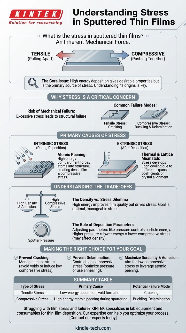
In sputtered thin films, stress is an inherent mechanical force that develops within the film during and after the deposition process. This internal force, which can be either tensile (pulling apart) or compressive (pushing together), is a critical factor that directly impacts the film's structural integrity, adhesion, and overall performance.
The core issue is that the very same high-energy deposition process that gives sputtered films their desirable density and adhesion is also the primary source of internal stress. Understanding the origins of this stress is the key to controlling it and preventing catastrophic film failure.
Why Stress is a Critical Concern
The Risk of Mechanical Failure
Excessive stress is the leading cause of mechanical failure in thin films. When internal forces exceed the film's structural limits or its adhesion to the substrate, the result is often failure.
Common Failure Modes
Tensile stress, which pulls the film's atoms apart, can lead to cracking. Conversely, high compressive stress, which pushes atoms together, can cause the film to buckle or delaminate from the substrate.
The Primary Causes of Stress in Sputtered Films
Stress in sputtered films originates from two distinct sources: the deposition process itself (intrinsic) and the interaction between the film and the substrate (extrinsic).
Intrinsic Stress: The Sputtering Process
This type of stress is built into the film as it grows. The dominant mechanism in sputtering is often called "atomic peening."
High-energy atoms and ions from the plasma bombard the growing film. This bombardment effectively forces atoms into the material's structure, creating a dense film but also generating significant compressive stress.
Extrinsic Stress: Material Mismatches
This stress develops after deposition, typically when the film cools down from the processing temperature to room temperature.
The two main causes are thermal mismatch and lattice mismatch. If the film and the substrate have different coefficients of thermal expansion, one will contract more than the other upon cooling, generating stress. Similarly, if their crystal structures do not align perfectly, it creates strain at the interface.
Understanding the Trade-offs
The Density vs. Stress Dilemma
The high-energy particle bombardment in sputtering is what produces films with excellent density, purity, and adhesion. However, this same energy is the primary driver of high compressive stress.
Reducing deposition energy to lower the stress can sometimes lead to less dense or more porous films, compromising their performance. The goal is not always zero stress, but an optimal level of manageable stress.
The Role of Deposition Parameters
Managing stress involves a careful balancing act. Adjusting parameters like sputter pressure can change the energy of bombarding particles. Higher pressure leads to more gas-phase collisions, reducing particle energy and thus lowering compressive stress, but it can also affect film density.
Making the Right Choice for Your Goal
Controlling stress requires tuning your deposition process and considering post-deposition treatments based on your specific goal.
- If your primary focus is preventing cracking: You need to manage tensile stress, which often means ensuring the process doesn't create voids or by inducing a low level of beneficial compressive stress.
- If your primary focus is preventing delamination: You must control high compressive stress by optimizing deposition pressure or using post-deposition annealing to relax the film.
- If your primary focus is maximizing durability and adhesion: Aim for a final state of low compressive stress, which leverages the atomic peening effect to create a dense film without risking mechanical failure.
Ultimately, mastering stress control is what separates a high-performance, reliable sputtered film from one that fails.
Summary Table:
| Type of Stress | Primary Cause | Potential Failure Mode |
|---|---|---|
| Tensile Stress | Low-energy deposition, void formation | Cracking |
| Compressive Stress | High-energy atomic peening during sputtering | Buckling, Delamination |
Struggling with film stress and failure? KINTEK specializes in lab equipment and consumables for thin-film deposition. Our expertise in sputtering technology can help you optimize your process parameters to achieve the ideal stress level for durable, high-performance films. Contact our experts today to discuss your specific application and ensure reliable results.
Visual Guide
Related Products
- Aluminized Ceramic Evaporation Boat for Thin Film Deposition
- Tungsten Evaporation Boat for Thin Film Deposition
- Electron Beam Evaporation Coating Oxygen-Free Copper Crucible and Evaporation Boat
- Molybdenum Tungsten Tantalum Evaporation Boat for High Temperature Applications
- Aluminum-Plastic Flexible Packaging Film for Lithium Battery Packaging
People Also Ask
- What are the alternatives to sputtering? Choose the Right Thin Film Deposition Method
- What is thin film deposition? Unlock Advanced Surface Engineering for Your Materials
- What is the chemical method for thin film deposition? Build Films from the Molecular Level Up
- Why is an alumina boat and Ti3AlC2 powder bed necessary for Ti2AlC sintering? Protect MAX Phase Purity
- What is the source of evaporation for thin film? Choosing Between Thermal and E-Beam Methods


