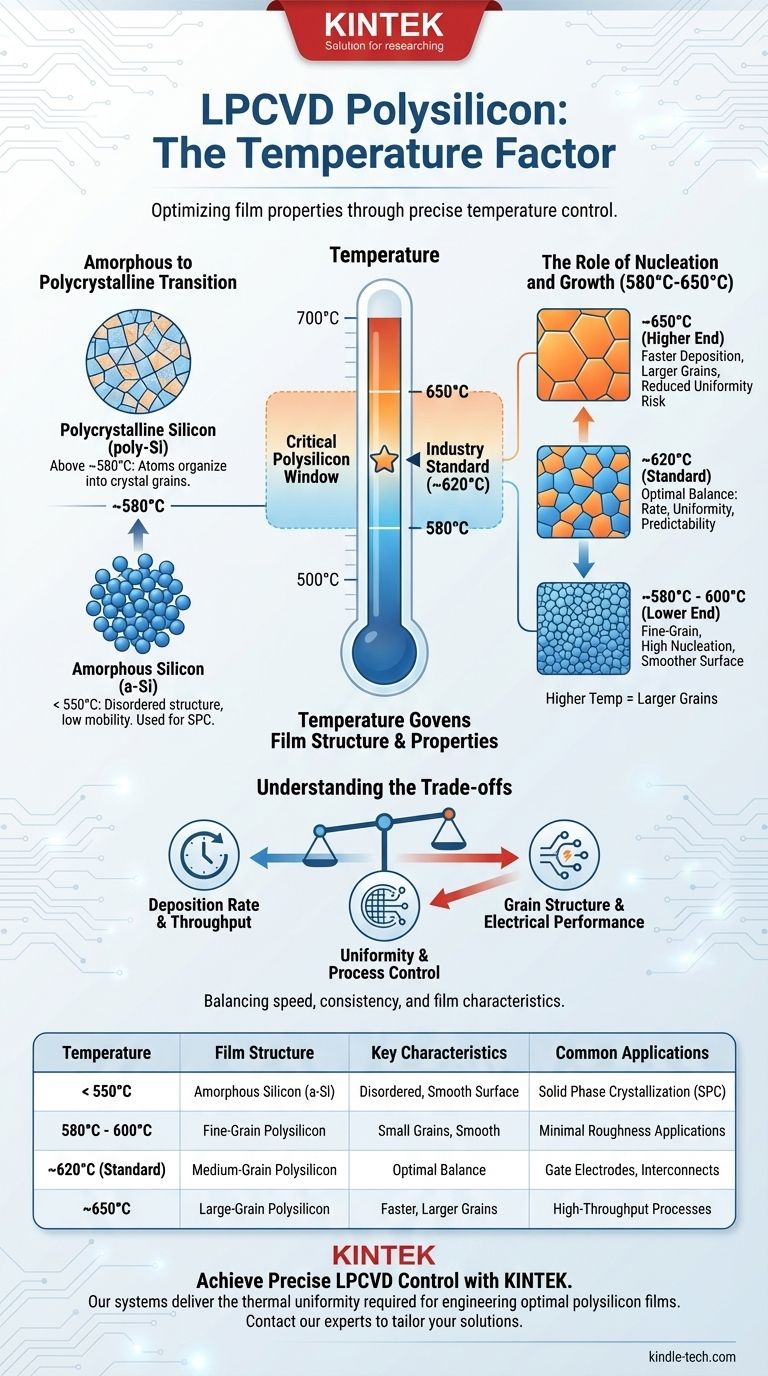
In a standard Low-Pressure Chemical Vapor Deposition (LPCVD) process, polysilicon is deposited at a temperature ranging from approximately 580°C to 650°C. This specific temperature window is not arbitrary; it is the critical parameter that determines the crystalline structure and resulting properties of the silicon film. The most common temperature used in production is around 620°C.
The deposition temperature in LPCVD is the primary control for the film's microstructure. It dictates whether the silicon forms as an amorphous or a polycrystalline layer, which in turn defines its electrical and mechanical characteristics for semiconductor device fabrication.
Why Temperature Governs the Film's Structure
The temperature inside an LPCVD furnace provides the thermal energy required to initiate and sustain the chemical reaction. For polysilicon, this typically involves the decomposition of a precursor gas like silane (SiH₄). However, its most crucial role is governing the mobility of the silicon atoms once they arrive on the wafer surface.
The Critical Transition Point
Atoms deposited on a surface will naturally try to arrange themselves into the lowest possible energy state, which is a crystal lattice. The process temperature determines if they have enough energy to do so.
- Below ~550°C: The silicon atoms lack sufficient thermal energy to move into ordered crystal sites before being buried by subsequent atoms. The result is a disordered, amorphous silicon (a-Si) film.
- Above ~580°C: Atoms possess enough energy to migrate on the surface and find a crystal lattice site. This allows for the formation of small, randomly oriented crystal domains known as grains, creating a polycrystalline silicon (poly-Si) film.
The Role of Nucleation and Growth
Within the polycrystalline range (580°C-650°C), temperature directly influences how crystal grains form and grow. This relationship dictates the final properties of the film.
Higher temperatures provide more energy, which generally leads to larger grain sizes. This is a critical factor, as grain boundaries can impede electron flow and act as trapping sites for dopant atoms.
The Impact of Specific Temperature Ranges
While the entire 580°C-650°C range produces polysilicon, small adjustments within this window are made to target specific film characteristics.
The Lower End: ~580°C - 600°C
Depositing at the lower end of the window results in a film with a very fine, small-grained structure. The nucleation rate is high compared to the grain growth rate.
The Industry Standard: ~620°C
This is the most common process temperature. It provides an optimal balance between a reasonable deposition rate for manufacturing throughput and excellent, predictable film properties. The resulting grain structure is well-understood and highly repeatable.
The Higher End: ~650°C
Pushing the temperature higher significantly increases the deposition rate. It also promotes larger grain growth. However, this comes at a cost, as the reaction can become too fast to control uniformly.
Understanding the Trade-offs
Choosing a specific temperature is an engineering decision that involves balancing competing factors.
Deposition Rate vs. Uniformity
A higher temperature means a faster deposition rate, which is good for productivity. However, if the reaction is too fast, the silane gas can be depleted before it reaches all the wafers in a large batch furnace, leading to poor thickness uniformity. The ~620°C range offers a manageable rate that ensures uniformity.
Grain Structure vs. Electrical Performance
Larger grains (from higher temperatures) generally result in a film with lower electrical resistivity after doping, as there are fewer grain boundaries to scatter charge carriers. However, the specific grain structure also impacts the film's stress and its behavior during subsequent etching or thermal processing steps.
Process Control vs. Throughput
While a 650°C process is faster, it is also more sensitive to variations. The reaction becomes "mass-transport limited," meaning the rate is limited by how fast gas can get to the surface. This makes the process harder to control compared to the "reaction-rate limited" regime at lower temperatures like 620°C.
Making the Right Choice for Your Goal
The ideal deposition temperature is determined by the end-use application of the polysilicon film.
- If your primary focus is standard gate electrodes or interconnects: A temperature around 620°C is the industry-proven standard, offering the best balance of predictable electrical properties, good uniformity, and efficient throughput.
- If your primary focus is a film with minimal surface roughness: Deposition at a lower temperature, between 580°C and 600°C, creates a finer grain structure that can be advantageous.
- If your primary focus is to create an amorphous film for later crystallization (Solid Phase Crystallization): You must deposit below the transition point, typically in the 530°C to 550°C range.
Ultimately, the precise deposition temperature is a strategic choice that directly engineers the fundamental properties of the polysilicon film to meet device requirements.
Summary Table:
| Temperature Range | Film Structure | Key Characteristics | Common Applications |
|---|---|---|---|
| < 550°C | Amorphous Silicon (a-Si) | Disordered structure, smooth surface | Solid Phase Crystallization (SPC) |
| 580°C - 600°C | Fine-Grain Polysilicon | Small grains, smooth surface | Applications requiring minimal roughness |
| ~620°C (Standard) | Medium-Grain Polysilicon | Optimal balance of rate and uniformity | Gate electrodes, interconnects |
| ~650°C | Large-Grain Polysilicon | Faster deposition, larger grains | High-throughput processes |
Need to optimize your LPCVD process for specific film properties? The precise temperature control of your deposition system is critical for achieving the desired polysilicon structure and performance. KINTEK specializes in high-performance lab equipment and consumables for semiconductor fabrication, offering solutions that deliver the thermal uniformity and process control your laboratory requires. Contact our experts today to discuss how our LPCVD systems and support can help you engineer polysilicon films tailored to your device specifications.
Visual Guide
Related Products
- 915MHz MPCVD Diamond Machine Microwave Plasma Chemical Vapor Deposition System Reactor
- Chemical Vapor Deposition CVD Equipment System Chamber Slide PECVD Tube Furnace with Liquid Gasifier PECVD Machine
People Also Ask
- What are the primary advantages of the CVD method for growing diamonds? Engineering High-Purity Gems and Components
- What pressure is needed for chemical vapor deposition of diamonds? Master the Low-Pressure 'Sweet Spot'
- How are CVD diamonds created? Discover the Science of Lab-Grown Diamond Precision
- How is a diamond formed from CVD? The Science of Growing Diamonds Atom by Atom
- What is microwave plasma CVD? A Guide to High-Purity Diamond and Material Synthesis

