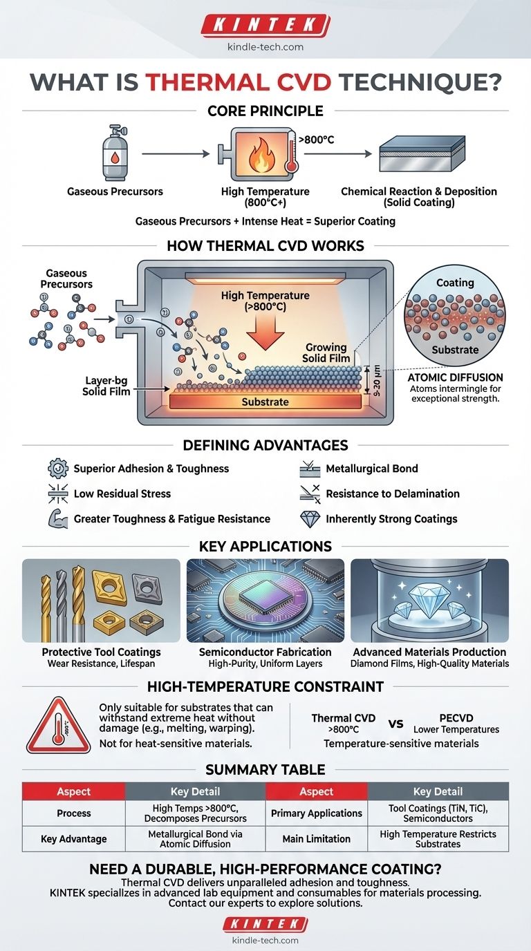
In essence, Thermal Chemical Vapor Deposition (CVD) is a materials processing technique that uses high temperatures to initiate a chemical reaction from gaseous precursors, resulting in the formation of a solid, high-performance coating on a substrate's surface. The process is prized for creating exceptionally tough and well-bonded films, primarily used for protective coatings on tooling and in semiconductor manufacturing.
Thermal CVD leverages intense heat to create a metallurgical bond between a coating and a substrate. This results in superior durability, but its high-temperature nature restricts its use to materials that can withstand the processing environment.
How Thermal CVD Works: A Matter of Heat and Chemistry
Thermal CVD is a process built on a straightforward principle: using thermal energy to drive a chemical reaction that deposits a solid material from a gas. The entire process takes place inside a controlled reaction chamber.
The Core Principle: Gaseous Precursors
First, one or more volatile gases, known as precursors, are introduced into the chamber. These gases contain the specific chemical elements required to form the final desired coating (e.g., titanium and carbon for a titanium carbide film).
The Role of High Temperature
The substrate—the part to be coated—is heated to a very high temperature, often exceeding 800°C. This intense heat is the catalyst; it provides the activation energy needed to break the chemical bonds within the precursor gas molecules.
Deposition and Film Growth
Once the precursor gases decompose near the hot substrate, the constituent atoms or molecules react and settle onto the surface. This deposition builds up, layer by layer, to form a dense, pure, and uniform solid film with a highly controlled thickness, typically between 5 and 20 μm.
The Defining Advantage: Superior Adhesion and Durability
The primary reason for choosing Thermal CVD over other methods is its ability to produce coatings with unparalleled adhesion and toughness. This is a direct result of the high temperatures involved.
The Power of Atomic Diffusion
The intense heat causes atoms from both the growing film and the substrate to intermingle at the interface. This atomic diffusion creates a graded, metallurgical bond rather than a distinct boundary.
This process is fundamentally different from a simple mechanical bond. It is more akin to welding two materials together at a microscopic level, resulting in an exceptionally strong connection that is highly resistant to delamination.
Resulting Material Properties
This superior bond contributes to several key performance benefits, including low residual stress, greater toughness, and excellent fatigue resistance. The coatings are inherently strong and resilient, not just a surface layer.
Where Thermal CVD Shines: Key Applications
The unique properties of Thermal CVD coatings make them ideal for specific, demanding applications where performance is critical.
Protective Tool Coatings
This is a primary application. Machine tools, cutting inserts, dies, and molds used in metal forming and injection molding are coated with materials like titanium nitride (TiN) or titanium carbide (TiC) to dramatically increase their wear resistance and lifespan.
Semiconductor Fabrication
In the semiconductor industry, Thermal CVD is used to deposit high-purity thin films of materials like silicon dioxide or polysilicon. The high temperature ensures a very clean and uniform layer, which is critical for fabricating integrated circuits.
Advanced Materials Production
The process is also used to create advanced, high-performance materials from scratch. A notable example is the production of synthetic diamonds, where carbon-containing gases are decomposed to grow high-quality diamond films.
Understanding the Trade-offs: The High-Temperature Constraint
While powerful, Thermal CVD is not a universal solution. Its greatest strength—high temperature—is also its most significant limitation.
The Substrate Limitation
The process is only suitable for substrates that can withstand the extreme heat without melting, warping, or losing their essential properties. For example, hardened steels can be softened and tempered by the heat, compromising the integrity of the underlying tool.
The Need for Alternatives
This limitation has driven the development of other deposition techniques. Methods like Plasma-Enhanced CVD (PECVD) operate at much lower temperatures, making them suitable for coating heat-sensitive materials like polymers, certain aluminum alloys, and pre-hardened components.
When to Choose Thermal CVD
Selecting the right deposition technology depends entirely on the material you are working with and your end goal.
- If your primary focus is maximum durability and adhesion: Thermal CVD is the gold standard for creating ultra-hard coatings on substrates (like carbide tools) that can tolerate the intense heat.
- If your primary focus is coating a temperature-sensitive material: You must look to lower-temperature alternatives, as Thermal CVD will likely damage or destroy your substrate.
- If your primary focus is achieving the highest purity and film quality: Thermal CVD is an excellent choice for applications like semiconductor layers or optical fibers where material perfection is paramount.
Ultimately, understanding the interplay between temperature and adhesion is the key to deciding if Thermal CVD is the right tool for your engineering challenge.
Summary Table:
| Aspect | Key Detail |
|---|---|
| Process | Uses high temperatures (>800°C) to decompose gaseous precursors for deposition. |
| Key Advantage | Creates a metallurgical bond via atomic diffusion for superior adhesion and toughness. |
| Primary Applications | Protective tool coatings (TiN, TiC), semiconductor films, synthetic diamond production. |
| Main Limitation | High temperature restricts use to substrates that can withstand the heat without damage. |
Need a Durable, High-Performance Coating for Your Tools or Components?
Thermal CVD delivers unparalleled adhesion and toughness for demanding applications. If your substrates can handle high temperatures, this is the gold-standard process for maximizing wear resistance and lifespan.
KINTEK specializes in advanced lab equipment and consumables for materials processing. Our expertise can help you determine if Thermal CVD is the right solution for your laboratory or production needs.
Contact our experts today to discuss your specific coating challenges and explore how our solutions can enhance your results.
Visual Guide
Related Products
- CVD Diamond for Thermal Management Applications
- HFCVD Machine System Equipment for Drawing Die Nano-Diamond Coating
- Multi Heating Zones CVD Tube Furnace Machine Chemical Vapor Deposition Chamber System Equipment
- Chemical Vapor Deposition CVD Equipment System Chamber Slide PECVD Tube Furnace with Liquid Gasifier PECVD Machine
- Customer Made Versatile CVD Tube Furnace Chemical Vapor Deposition Chamber System Equipment
People Also Ask
- Are CVD diamonds real or fake? Discover the Truth About Lab-Grown Diamonds
- Will a CVD diamond pass a diamond tester? Yes, because it's a real diamond.
- What are the optical properties of CVD diamond? Unlock Unmatched Performance for Demanding Applications
- How long does it take to make a CVD diamond? A Detailed Look at the Growth Timeline
- How do they make diamonds in CVD? Unlock the Secrets of Lab-Grown Diamond Creation