Knowledge What is the thickness of a film? A Guide to the 1mm Threshold and Measurement Units
Author avatar

Tech Team · Kintek Solution

Updated 2 weeks ago

What is the thickness of a film? A Guide to the 1mm Threshold and Measurement Units

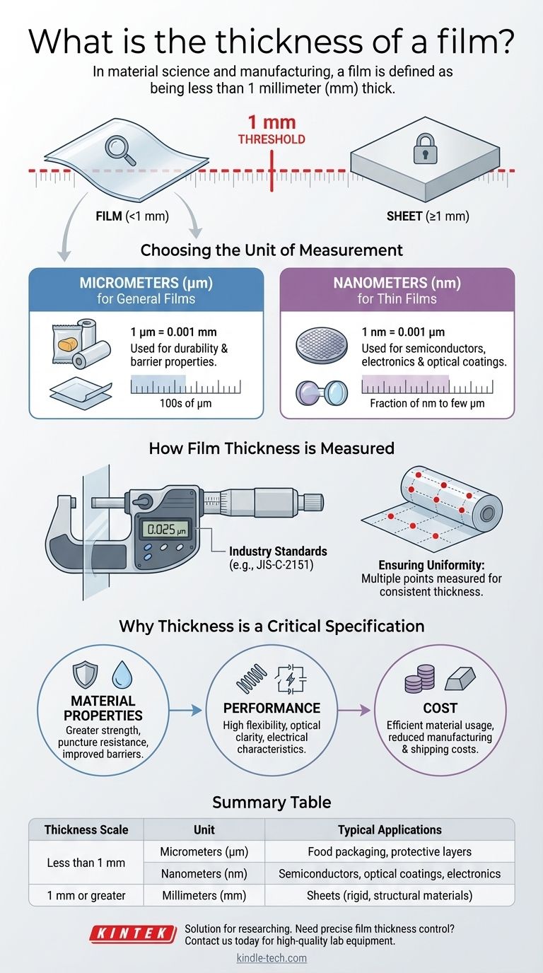
In material science and manufacturing, the thickness of a film is defined as being less than 1 millimeter (mm). This thickness can range from several micrometers (µm) for common applications down to fractions of a nanometer (nm) for highly specialized "thin films," such as those used in electronics or optics.

The term "film" fundamentally describes a material layer thinner than 1 mm, which distinguishes it from a thicker "sheet." The specific unit of measurement used—micrometers or nanometers—is determined entirely by the film's application and required precision.

Defining the Scale: Film vs. Sheet

The distinction between a film and a sheet is not arbitrary; it's a critical industry classification based on a simple threshold.

The 1 Millimeter Rule

The most important defining characteristic is the 1 mm threshold. Any material layer that is 1 mm or thicker is properly referred to as a sheet.

If the material is less than 1 mm thick, it is classified as a film. This rule provides a clear and universal standard for material specification.

Why This Distinction Matters

This classification directly impacts expectations about the material's properties. Films are expected to have a high degree of flexibility, while sheets are associated with rigidity and structural integrity.

Choosing the Right Unit of Measurement

The unit used to express a film's thickness communicates the scale and precision of the application.

Micrometers (µm) for General Films

For most industrial and commercial films, such as food packaging or protective layers, thickness is measured in micrometers (µm).

One micrometer is one-thousandth of a millimeter (0.001 mm). This unit provides the right level of granularity for applications where durability and barrier properties are key.

Nanometers (nm) for Thin Films

For advanced technological applications, the term "thin film" is used. These are layers of material ranging from a few micrometers down to a single layer of atoms.

The thickness of these highly engineered films is measured in nanometers (nm). One nanometer is one-thousandth of a micrometer (0.001 µm), making it the appropriate scale for semiconductors, optical coatings, and other precision surfaces.

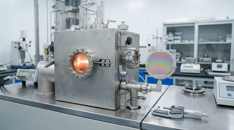
How Film Thickness is Measured

Ensuring a film meets its specified thickness is a critical part of quality control.

The Micrometer Method

The most common method for measuring general film thickness is with a specialized instrument called a micrometer.

Industry standards, such as JIS-C-2151, outline the precise procedures for using this tool to get accurate and repeatable results.

Ensuring Uniformity

A single measurement is insufficient. To guarantee quality, technicians take measurements at multiple specified points across both the length and width of the film.

This process ensures the film has a consistent and uniform thickness, which is crucial for predictable performance.

Why Thickness is a Critical Specification

The thickness of a film is not just a number; it is a primary driver of its function, performance, and cost.

Impact on Material Properties

Thicker films generally provide greater tensile strength, puncture resistance, and improved barrier properties against moisture or gases.

Impact on Performance

Thinner films are often required for applications demanding high flexibility, optical clarity, or specific electrical characteristics. In electronics, the precise thickness of a thin film can determine a component's conductive or insulating properties.

Impact on Cost

Material usage is a primary cost driver. Producing a film that is thicker than necessary wastes raw material and increases manufacturing and shipping costs. Precise thickness control is essential for economic efficiency.

Making the Right Choice for Your Goal

To interpret a specification correctly, you must consider the context of the application.

  • If your primary focus is packaging or industrial materials: You will almost always be working with specifications in micrometers (µm).
  • If your primary focus is electronics, optics, or semiconductors: You will be dealing with "thin films" where thickness is measured in the much finer scale of nanometers (nm).
  • If your primary focus is differentiating from thicker materials: Remember the key threshold: anything 1 mm or thicker is classified as a "sheet," not a film.

Understanding these fundamental distinctions in scale and terminology is the first step to accurately specifying and evaluating material performance.

Summary Table:

Thickness Scale Unit Typical Applications
Less than 1 mm Micrometers (µm) Food packaging, protective layers
Less than 1 mm Nanometers (nm) Semiconductors, optical coatings, electronics
1 mm or greater Millimeters (mm) Sheets (rigid, structural materials)

Need precise film thickness control for your lab? KINTEK specializes in high-quality lab equipment and consumables for accurate material analysis and production. Whether you're developing thin films for electronics or require consistent packaging materials, our solutions ensure reliability and efficiency. Contact us today to discuss how we can support your laboratory's specific needs!

Related Products

People Also Ask

Related Products

RF PECVD System Radio Frequency Plasma-Enhanced Chemical Vapor Deposition RF PECVD

RF PECVD System Radio Frequency Plasma-Enhanced Chemical Vapor Deposition RF PECVD

RF-PECVD is an acronym for "Radio Frequency Plasma-Enhanced Chemical Vapor Deposition." It deposits DLC (Diamond-like carbon film) on germanium and silicon substrates. It is utilized in the 3-12um infrared wavelength range.

Chemical Vapor Deposition CVD Equipment System Chamber Slide PECVD Tube Furnace with Liquid Gasifier PECVD Machine

Chemical Vapor Deposition CVD Equipment System Chamber Slide PECVD Tube Furnace with Liquid Gasifier PECVD Machine

KT-PE12 Slide PECVD System: Wide power range, programmable temp control, fast heating/cooling with sliding system, MFC mass flow control & vacuum pump.

Molybdenum Tungsten Tantalum Evaporation Boat for High Temperature Applications

Molybdenum Tungsten Tantalum Evaporation Boat for High Temperature Applications

Evaporation boat sources are used in thermal evaporation systems and are suitable for depositing various metals, alloys and materials. Evaporation boat sources are available in different thicknesses of tungsten, tantalum and molybdenum to ensure compatibility with a variety of power sources. As a container, it is used for vacuum evaporation of materials. They can be used for thin film deposition of various materials, or designed to be compatible with techniques such as electron beam fabrication.

Hemispherical Bottom Tungsten Molybdenum Evaporation Boat

Hemispherical Bottom Tungsten Molybdenum Evaporation Boat

Used for gold plating, silver plating, platinum, palladium, suitable for a small amount of thin film materials. Reduce the waste of film materials and reduce heat dissipation.

Aluminized Ceramic Evaporation Boat for Thin Film Deposition

Aluminized Ceramic Evaporation Boat for Thin Film Deposition

Vessel for depositing thin films; has an aluminum-coated ceramic body for improved thermal efficiency and chemical resistance. making it suitable for various applications.

Tungsten Evaporation Boat for Thin Film Deposition

Tungsten Evaporation Boat for Thin Film Deposition

Learn about tungsten boats, also known as evaporated or coated tungsten boats. With a high tungsten content of 99.95%, these boats are ideal for high-temperature environments and widely used in various industries. Discover their properties and applications here.

Ceramic Evaporation Boat Set Alumina Crucible for Laboratory Use

Ceramic Evaporation Boat Set Alumina Crucible for Laboratory Use

It can be used for vapor deposition of various metals and alloys. Most metals can be evaporated completely without loss. Evaporation baskets are reusable.1

VHP Sterilization Equipment Hydrogen Peroxide H2O2 Space Sterilizer

VHP Sterilization Equipment Hydrogen Peroxide H2O2 Space Sterilizer

A hydrogen peroxide space sterilizer is a device that uses vaporized hydrogen peroxide to decontaminate enclosed spaces. It kills microorganisms by damaging their cellular components and genetic material.

Electron Beam Evaporation Coating Conductive Boron Nitride Crucible BN Crucible

Electron Beam Evaporation Coating Conductive Boron Nitride Crucible BN Crucible

High-purity and smooth conductive boron nitride crucible for electron beam evaporation coating, with high temperature and thermal cycling performance.

High Performance Laboratory Freeze Dryer

High Performance Laboratory Freeze Dryer

Advanced lab freeze dryer for lyophilization, preserving biological & chemical samples efficiently. Ideal for biopharma, food, and research.

E Beam Crucibles Electron Gun Beam Crucible for Evaporation

E Beam Crucibles Electron Gun Beam Crucible for Evaporation

In the context of electron gun beam evaporation, a crucible is a container or source holder used to contain and evaporate the material to be deposited onto a substrate.

High Performance Laboratory Freeze Dryer for Research and Development

High Performance Laboratory Freeze Dryer for Research and Development

Advanced laboratory freeze dryer for lyophilization, preserving sensitive samples with precision. Ideal for biopharmaceuticals, research & food industries.

Variable Speed Peristaltic Pump

Variable Speed Peristaltic Pump

KT-VSP Series Smart Variable Speed Peristaltic Pumps offer precise flow control for labs, medical, and industrial applications. Reliable, contamination-free liquid transfer.

Single Punch Electric Tablet Press Machine Laboratory Powder Tablet Punching TDP Tablet Press

Single Punch Electric Tablet Press Machine Laboratory Powder Tablet Punching TDP Tablet Press

The single-punch electric tablet press is a laboratory-scale tablet press suitable for corporate laboratories in pharmaceutical, chemical, food, metallurgical and other industries.

Square Bidirectional Pressure Mold for Lab Use

Square Bidirectional Pressure Mold for Lab Use

Discover precision in molding with our Square Bidirectional Pressure Mold. Ideal for creating diverse shapes and sizes, from squares to hexagons, under high pressure and uniform heating. Perfect for advanced material processing.

Ball Press Mold for Lab

Ball Press Mold for Lab

Explore versatile Hydraulic Hot Press molds for precise compression molding. Ideal for creating various shapes and sizes with uniform stability.

Circulating Water Vacuum Pump for Laboratory and Industrial Use

Circulating Water Vacuum Pump for Laboratory and Industrial Use

Efficient circulating water vacuum pump for labs - oil-free, corrosion-resistant, quiet operation. Multiple models available. Get yours now!

Square Lab Press Mold for Laboratory Applications

Square Lab Press Mold for Laboratory Applications

Create uniform samples easily with Square Lab Press Mold - available in various sizes. Ideal for battery, cement, ceramics, and more. Custom sizes available.

Polygon Press Mold for Lab

Polygon Press Mold for Lab

Discover precision polygon press molds for sintering. Ideal for pentagon-shaped parts, our molds ensure uniform pressure and stability. Perfect for repeatable, high-quality production.

Cylindrical Lab Electric Heating Press Mold for Laboratory Applications

Cylindrical Lab Electric Heating Press Mold for Laboratory Applications

Efficiently prepare samples with Cylindrical Lab Electric Heating Press Mold. Fast heating, high temp & easy operation. Custom sizes available. Perfect for battery, ceramic & biochemical research.


Leave Your Message