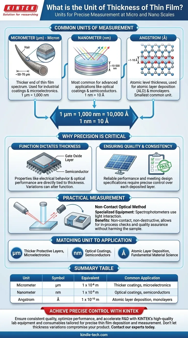
The thickness of a thin film is most commonly measured in nanometers (nm), micrometers (µm), and angstroms (Å). The specific unit chosen depends entirely on the thickness of the layer and the precision required for its application, which can range from a single layer of atoms to thousands of atomic layers thick.
The unit used for thin film thickness is not singular; it is chosen to match the scale of the application. The critical insight is that these measurements reflect a scale where even minuscule variations in thickness can drastically alter a material's fundamental properties.
Understanding the Scale of Thin Film Units
To work with thin films, you must first develop an intuition for the incredibly small scales involved. The units are chosen to make the numbers manageable and meaningful for a given context.
The Micrometer (µm)
A micrometer, also known as a micron, is one-millionth of a meter. This unit is typically used for the "thicker" end of the thin film spectrum.
Many industrial coatings or layers in microelectronic devices are measured in micrometers. For context, a typical human hair is about 50-70 µm in diameter.
The Nanometer (nm)
The nanometer is the most frequently used unit for advanced thin film applications, such as optical coatings and semiconductor devices. One nanometer is one-billionth of a meter.
There are 1,000 nanometers in one micrometer. A film described as 0.5 µm thick is identical to one that is 500 nm thick.
The Angstrom (Å)
The angstrom is the smallest of the common units, representing one-tenth of a nanometer (or one ten-billionth of a meter).
This unit is used when discussing thicknesses at the atomic level, such as in atomic layer deposition or when describing a monolayer (a single layer of atoms). There are 10 angstroms in one nanometer.
Why This Precision is Critical
Measuring thin film thickness is not an academic exercise; it is essential for controlling the final product's function and performance.
Function Dictates Thickness
The physical, optical, and electrical properties of a thin film are directly tied to its thickness.
For an optical coating on a lens, a difference of just a few nanometers can change which wavelengths of light are reflected or transmitted, altering the color and performance. In semiconductors, the thickness of gate oxides determines the device's electrical behavior.
Ensuring Quality and Consistency
To manufacture products with reliable performance, from solar panels to microchips, the thickness of each deposited layer must be precisely controlled.
Accurate measurement ensures that every product meets its design specifications and functions optimally.
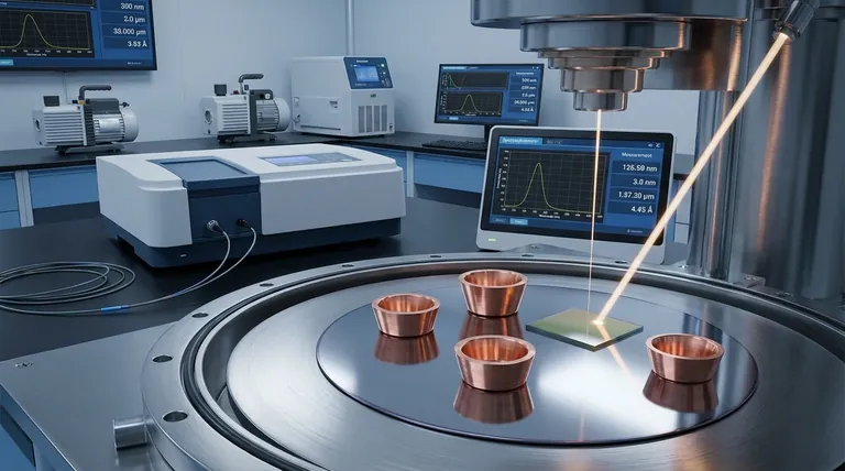
The Practicalities of Measurement
Given the microscopic scale, specialized equipment is required to measure thin film thickness accurately without damaging the sample.
Non-Contact Optical Methods
Tools like spectrophotometers are widely used because they are non-contact and non-destructive. They analyze how light interacts with the film to calculate its thickness.
This optical approach is crucial for in-process checks and quality control, as it doesn't harm the delicate component being measured.
The Value of Non-Destructive Testing
The ability to measure a film without touching or destroying it is paramount. It allows for quality assurance on finished products and real-time monitoring during the deposition process itself.
Matching the Unit to the Application
Your choice of unit simply reflects the world you are working in. Use this as your guide:
- If your primary focus is on optical coatings or semiconductors: You will primarily work in nanometers (nm), as precise control at this level determines the film's functional properties.
- If your primary focus is on thicker protective layers or microelectronics: Micrometers (µm or microns) will be your standard unit of measurement.
- If your primary focus is on atomic layer deposition or fundamental materials science: You will encounter angstroms (Å) to describe thicknesses approaching a single layer of atoms.
Understanding this scale is the first step toward controlling the unique physical properties that emerge in thin films.
Summary Table:
| Unit | Symbol | Equivalent | Common Application |
|---|---|---|---|
| Micrometer | µm | 1 x 10⁻⁶ m | Thicker coatings, microelectronics |
| Nanometer | nm | 1 x 10⁻⁹ m | Optical coatings, semiconductors |
| Angstrom | Å | 1 x 10⁻¹⁰ m | Atomic layer deposition, monolayers |
Achieve precise control over your thin film processes with KINTEK.
Whether you are developing advanced optical coatings, semiconductor devices, or protective layers, the accuracy of your film's thickness is paramount. KINTEK specializes in providing high-quality lab equipment and consumables tailored for precise thin film deposition and measurement.
Our solutions help you ensure consistent quality, optimize performance, and accelerate your R&D and production. Don't let thickness variations compromise your product's functionality.
Contact our experts today to discuss how KINTEK can support your laboratory's specific thin film needs.
Visual Guide
Related Products
- Custom PTFE Teflon Parts Manufacturer for PTFE Measuring Cylinder 10/50/100ml
- Small Lab Rubber Calendering Machine
- Battery Lab Equipment 304 Stainless Steel Strip Foil 20um Thick for Battery Test
People Also Ask
- What role do standard pyrometric cones (PCE Cones) play during refractoriness testing? Ensure High-Temp Stability
- What chemicals are used in heat treatment? Master the Quenching Process for Optimal Metal Properties
- What is the best solvent for FTIR? Master Solvent Selection for Clear, Accurate Spectra
- How is PTFE utilized for insulation in Alloy 22 corrosion setups? Ensure Signal Purity & Accuracy
- What are the disadvantages of flash pyrolysis oil? Overcoming Key Challenges in Bio-Oil Utilization