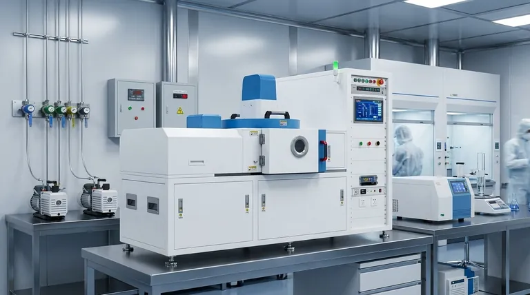
At its core, RF magnetron sputtering is a physical vapor deposition (PVD) technique used to create ultra-thin films. It uses a combination of an inert gas plasma, a powerful magnetic field, and a radio-frequency (RF) power source to eject atoms from a source material (the "target") and deposit them onto a surface (the "substrate"). This process is uniquely capable of depositing non-conductive, or insulating, materials.
The fundamental problem RF magnetron sputtering solves is the inability of simpler DC sputtering systems to deposit insulating materials. By using an alternating RF electric field, it prevents a process-killing charge buildup on the target, making it a versatile tool for creating advanced ceramic and oxide films.
The Foundation: How Sputtering Works
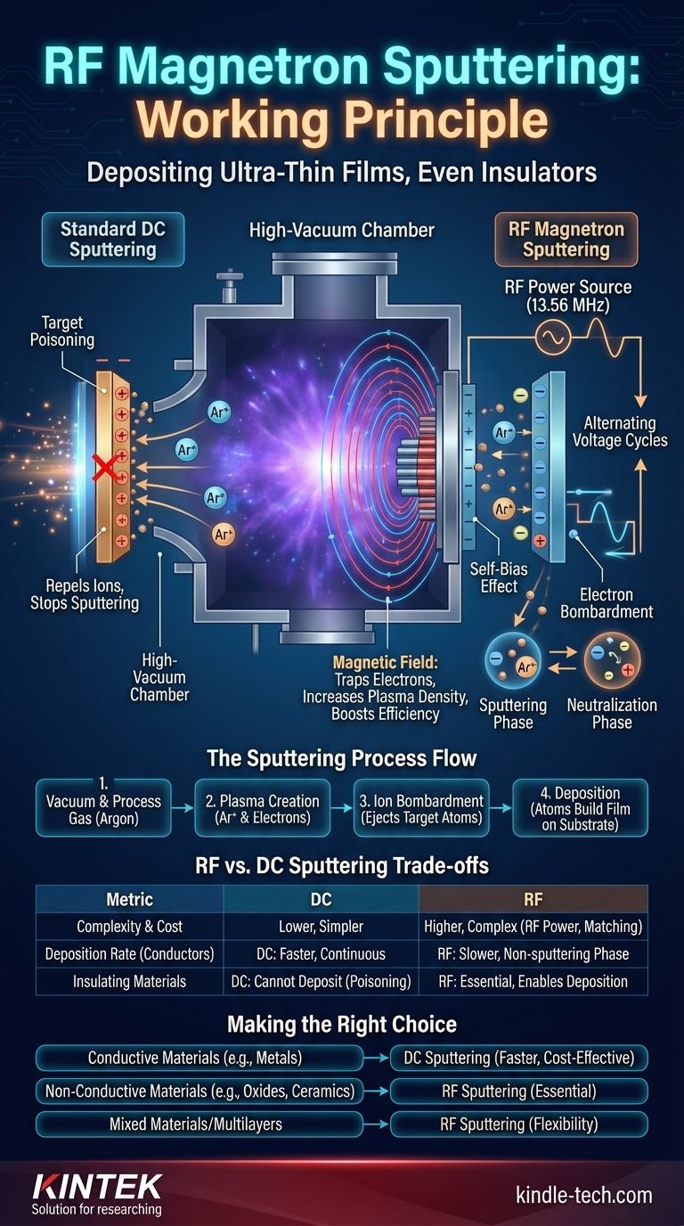
To understand the "RF" and "magnetron" components, we must first grasp the basic principle of sputtering. The entire process takes place inside a high-vacuum chamber.
The Vacuum and Process Gas
First, the chamber is pumped down to a very low pressure to remove contaminants. Then, a small, precisely controlled amount of an inert gas, typically argon (Ar), is introduced.
Creating the Plasma
A high voltage is applied across the chamber, with the target material acting as the cathode (negative) and the substrate holder or chamber walls as the anode (positive). This strong electric field energizes the argon gas, stripping electrons from the argon atoms and creating a plasma—an ionized gas consisting of positive argon ions (Ar+) and free electrons.
Bombardment and Deposition
The positively charged argon ions are forcefully accelerated toward the negatively charged target. They collide with the target surface with such high energy that they physically knock out, or "sputter," atoms of the target material. These sputtered atoms then travel through the vacuum and condense on the substrate, gradually building up a thin film.
The "Magnetron" Enhancement: Boosting Efficiency
Standard sputtering is slow. Magnetron sputtering dramatically increases the speed and efficiency of this process by adding a critical component: a magnetic field.
The Role of the Magnetic Field
A set of strong permanent magnets is placed behind the target. This creates a magnetic field that is parallel to the target's surface.
Trapping Electrons for Denser Plasma
This magnetic field has a profound effect on the light, negatively charged electrons in the plasma. It traps them in a spiral, or cycloidal, path directly in front of the target. By confining the electrons, their path length is greatly increased, which massively raises the probability that they will collide with and ionize neutral argon atoms.
The Result: Faster Deposition Rates
This enhanced ionization creates a much denser plasma concentrated near the target. More argon ions mean more bombardment, which in turn leads to a significantly higher rate of atoms being sputtered from the target. The result is a much faster and more efficient film deposition.
The "RF" Solution: Sputtering Insulators
While magnetron sputtering is highly efficient, it hits a wall when the target material is an electrical insulator, like a ceramic or an oxide. This is where the radio-frequency (RF) power source becomes essential.
The Challenge with DC Sputtering
In a standard DC system, as positive argon ions strike an insulating target, they cannot be neutralized because the material doesn't conduct electricity. This leads to a rapid buildup of positive charge on the target's surface. This positive layer, known as "target poisoning," repels the incoming positive argon ions, quickly extinguishing the plasma and halting the sputtering process entirely.
How the RF Field Works
Instead of a constant DC voltage, an RF power source applies an alternating voltage that oscillates millions of times per second (typically at 13.56 MHz).
During one half of the cycle, the target is negative, attracting the positive argon ions for sputtering just like in the DC process.
Crucially, during the other half of the cycle, the target becomes positive. In this brief moment, it attracts the highly mobile electrons from the plasma, which effectively neutralize the positive charge that built up during the sputtering half-cycle.
The "Self-Bias" Effect
Because electrons are much lighter and more mobile than argon ions, far more electrons reach the target during its positive half-cycle than ions do during the negative half-cycle. This imbalance results in the target developing a net negative charge, or a "self-bias," which is essential for maintaining the ion bombardment needed for sputtering.
Understanding the Trade-offs
While powerful, RF magnetron sputtering is not always the best choice. It involves clear trade-offs compared to its simpler DC counterpart.
Complexity and Cost
RF power supplies, impedance-matching networks, and shielding are significantly more complex and expensive than DC power systems. This makes the initial equipment investment higher.
Deposition Rates
For depositing conductive materials like metals, DC magnetron sputtering is often faster and more efficient. The RF cycle includes a "non-sputtering" phase (the electron bombardment phase), which can slightly reduce the overall deposition rate compared to a continuous DC process.
Process Control
The RF field provides additional parameters for tuning the plasma's characteristics. This offers greater control over film properties like stress and density but also adds a layer of complexity to process development.
Making the Right Choice for Your Goal
Selecting the correct sputtering technique depends entirely on the material you need to deposit.
- If your primary focus is depositing conductive materials (like metals or transparent conductors): DC magnetron sputtering is almost always the more cost-effective and faster choice.
- If your primary focus is depositing non-conductive materials (like oxides, nitrides, or ceramics): RF magnetron sputtering is the essential and correct technique to overcome target poisoning.
- If your primary focus is depositing a mix of materials or creating complex multilayer stacks: An RF system provides the ultimate flexibility to handle both conductive and insulating layers within the same process.
By understanding these core principles, you can confidently select and optimize the sputtering process that directly aligns with your material and application goals.
Summary Table:
| Component | Role in the Process | Key Benefit |
|---|---|---|
| RF Power (13.56 MHz) | Alternates voltage to neutralize charge buildup on insulating targets. | Enables deposition of non-conductive materials (e.g., Al₂O₃, SiO₂). |
| Magnetic Field | Traps electrons near the target to create a dense plasma. | Increases ionization for faster, more efficient deposition rates. |
| Inert Gas (Argon) | Ionized to form plasma; ions bombard the target to eject atoms. | Provides the energetic particles necessary for the sputtering process. |
| High Vacuum Chamber | Creates a clean, contaminant-free environment for the process. | Ensures high-purity, high-quality thin film deposition. |
Ready to integrate RF magnetron sputtering into your lab's capabilities?
KINTEK specializes in providing high-performance lab equipment and consumables for advanced thin-film deposition. Whether you are developing next-generation semiconductors, optical coatings, or protective ceramic layers, our expertise ensures you have the right tools for precise and reliable results.
Contact our experts today to discuss how our sputtering solutions can enhance your research and development process.
Visual Guide
Related Products
People Also Ask
- What is plasma enhanced chemical vapour deposition process? Unlock Low-Temperature, High-Quality Thin Films
- What is plasma chemical vapor deposition? A Low-Temperature Thin Film Coating Solution
- What is the role of RF-PECVD in VFG preparation? Mastering Vertical Growth and Surface Functionality
- What is an example of PECVD? RF-PECVD for High-Quality Thin Film Deposition
- How does plasma enhance CVD? Unlock Low-Temperature, High-Quality Film Deposition
