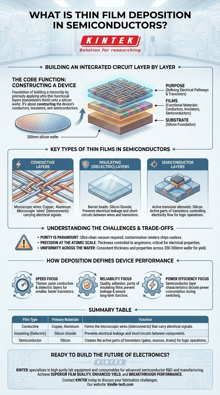
In the context of semiconductors, thin film deposition is the foundational process of building an integrated circuit by precisely applying ultra-thin, functional layers of material onto a silicon wafer. These layers, often just nanometers thick, are not merely coatings; they are the patterned conductors, insulators, and semiconductors that collectively form the transistors and wiring of a modern microchip.
The central concept to grasp is that thin film deposition is not about protecting a surface, but about constructing a device. It is the microscopic equivalent of building a skyscraper floor by floor, where each layer has a specific material and purpose required for the final structure to function.
The Core Function: Building Circuits Layer by Layer
To understand the role of deposition, it's best to think of it as a highly controlled construction process. A microchip is an incredibly complex, three-dimensional structure built from the ground up on a flat base.
The Substrate: The Silicon Foundation
All semiconductor manufacturing begins with a substrate, which is typically a highly pure, polished disc of silicon known as a wafer. This wafer serves as the stable foundation upon which all other circuit elements are built.
The Films: Creating Functional Materials
The "thin films" are the active materials deposited onto this wafer. These aren't just one type of material; they are a sequence of different materials, each chosen for its specific electrical properties.
The Purpose: Defining Electrical Pathways
Each layer is meticulously patterned to form specific parts of the circuit. By depositing layers of conductive, insulating, and semiconducting materials in a precise sequence, engineers construct the millions or billions of individual transistors that make up a processor or memory chip.
Key Types of Thin Films in Semiconductors
Different materials are deposited to perform three critical functions within an integrated circuit. The ability to precisely deposit and shape these films is what enables modern electronics.
Conductive Layers
These films are typically made of metals like copper or aluminum. They act as the microscopic "wires" or interconnects that carry electrical signals between different transistors and other components on the chip.
Insulating (Dielectric) Layers
Materials like silicon dioxide are deposited to act as insulators. Their primary role is to prevent electrical current from leaking or short-circuiting between the densely packed wires and transistors, ensuring signals go only where they are intended.
Semiconductor Layers
Specialized deposition techniques are used to add or modify layers of semiconductor material, like silicon itself. These layers form the active parts of the transistor—the gates, sources, and drains—that control the flow of electricity, performing the logic operations at the heart of computing.
Understanding the Challenges and Trade-offs
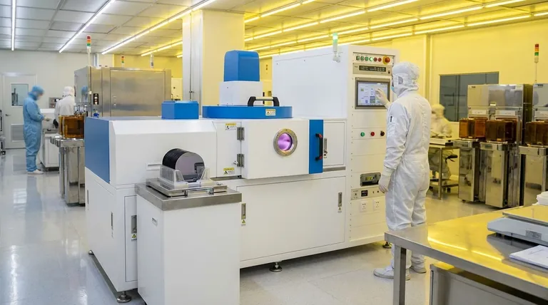
The concept of depositing a thin layer sounds simple, but performing it at the scale required for modern semiconductors presents immense technical challenges. The success of the entire chip manufacturing process hinges on overcoming them.
Purity is Paramount
The deposition environment must be an ultra-clean vacuum. A single microscopic dust particle or impurity atom can contaminate a layer, causing a short circuit and rendering an entire chip useless.
Precision at the Atomic Scale
The electrical properties of a transistor are highly dependent on the exact thickness of its insulating and semiconductor layers. Deposition processes must be controlled with a precision of just a few angstroms—sometimes equivalent to a single layer of atoms.
Uniformity Across the Wafer
The deposited film must have the exact same thickness and material properties across the entire surface of the 200mm or 300mm wafer. Any variation could cause the chips from one side of the wafer to perform differently than those from the other, leading to low manufacturing yields.
How Deposition Defines Device Performance
Ultimately, the choice and quality of thin film deposition techniques directly impact the final product. Understanding this connection is key to appreciating its importance.
- If your primary focus is processing speed: Achieving thinner, purer conductive films and ultra-thin, high-performance dielectric layers is essential for making transistors smaller and faster.
- If your primary focus is device reliability: The quality, adhesion, and purity of insulating films are critical for preventing electrical leakage and ensuring the chip functions correctly for years without failure.
- If your primary focus is power efficiency: The characteristics of the deposited semiconductor layers in the transistor dictate how much power is consumed during switching, a crucial factor for mobile devices.
Thin film deposition is the atomic-level architecture that turns a simple slice of silicon into a powerful computational device.
Summary Table:
| Film Type | Primary Materials | Function in a Semiconductor |
|---|---|---|
| Conductive | Copper, Aluminum | Forms the microscopic wires (interconnects) that carry electrical signals. |
| Insulating (Dielectric) | Silicon Dioxide | Prevents electrical leakage and short-circuits between components. |
| Semiconductor | Silicon | Creates the active parts of transistors (gates, sources, drains) for logic operations. |
Ready to Build the Future of Electronics?
The precision and reliability of your thin film deposition process are fundamental to your semiconductor's performance, yield, and innovation. KINTEK specializes in providing the high-purity lab equipment and consumables essential for advanced semiconductor R&D and manufacturing.
Let us help you achieve:
- Superior Film Quality: Ensure the purity, uniformity, and atomic-scale precision your devices demand.
- Enhanced Yield: Minimize defects and contamination with reliable equipment and materials.
- Breakthrough Performance: Access the tools needed to develop next-generation chips with faster speeds and lower power consumption.
Contact KINTEK today to discuss how our solutions can support your specific semiconductor fabrication challenges. #ContactForm
Visual Guide
Related Products
- Aluminized Ceramic Evaporation Boat for Thin Film Deposition
- Tungsten Evaporation Boat for Thin Film Deposition
- Electron Beam Evaporation Coating Oxygen-Free Copper Crucible and Evaporation Boat
- Molybdenum Tungsten Tantalum Evaporation Boat for High Temperature Applications
- HFCVD Machine System Equipment for Drawing Die Nano-Diamond Coating
People Also Ask
- What are the alternatives to sputtering? Choose the Right Thin Film Deposition Method
- What is thin film deposition? Unlock Advanced Surface Engineering for Your Materials
- Why are high-purity ceramic boats used for lignin activation? Ensure Purity & Thermal Stability
- What are the applications of thin films deposition? Unlock New Possibilities for Your Materials
- What is the widely used boat made of in thermal evaporation? Choosing the Right Material for High-Purity Deposition


