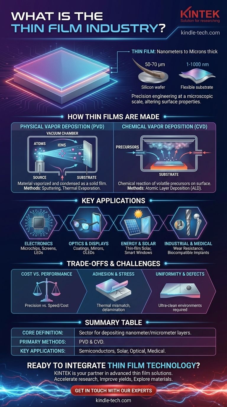
In essence, the thin film industry is the sector of technology and manufacturing dedicated to depositing exceptionally thin layers of material onto a surface, known as a substrate. These layers, often ranging from a few atoms to several micrometers thick, are engineered to fundamentally alter the substrate's physical, electrical, optical, or chemical properties, enabling the creation of advanced products like microchips, solar panels, and specialized optical lenses.
The thin film industry should not be seen as a market for a single product. Instead, it is a foundational enabling technology that gives materials new capabilities, making it a critical, often invisible, component behind countless modern innovations.
What Constitutes a "Thin Film"?
To understand the industry, we must first define its core product. A thin film is not merely a coat of paint; it is a feat of precision engineering at a microscopic scale.
From Nanometers to Microns
A thin film's thickness is its defining characteristic, typically measured in nanometers (billionths of a meter) or micrometers (millionths of a meter). For context, a single human hair is about 50-70 micrometers thick, meaning many thin films can be thousands of times thinner.
The Substrate: The Foundation
The film is always deposited onto a substrate, which is the base material or object. Substrates can be rigid, like the silicon wafers used for computer chips or the glass in architectural windows, or flexible, like the plastic used in some modern displays and solar cells.
The Purpose: Modifying Properties
The goal is to impart new functions. A thin film can make a material electrically conductive or insulating, change how it reflects or transmits light, make it resistant to corrosion and wear, or give it biocompatible properties for medical implants.
The Core Technologies: How Thin Films Are Made
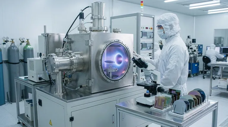
The methods used to create these films are highly controlled processes that typically occur in a vacuum. They are broadly divided into two main categories.
Physical Vapor Deposition (PVD)
PVD encompasses methods where a material is turned into a vapor through physical means, transported through a vacuum or low-pressure environment, and then condensed onto the substrate as a solid film.
Think of it like boiling water and watching steam (vapor) condense on a cold mirror. Common PVD techniques include sputtering, which uses ions to eject atoms from a source material, and thermal evaporation, which uses heat to boil the material into a vapor.
Chemical Vapor Deposition (CVD)
In CVD, the substrate is exposed to one or more volatile chemical precursors, which react or decompose on the substrate's surface to produce the desired film.
This is more like the formation of frost on a window pane, where water vapor in the air chemically transforms into a solid layer of ice crystals upon contact with the cold surface. CVD is prized for creating highly pure and uniform films. A key variant is Atomic Layer Deposition (ALD), which builds films one single atomic layer at a time, offering unparalleled precision.
Where the Thin Film Industry is Essential
The applications of thin film technology are vast and are integral to many of the world's most important industries.
Electronics and Semiconductors
This is the largest and most well-known application. The microscopic circuits on a microchip are built by depositing alternating layers of conductive, insulating, and semiconducting thin films onto a silicon wafer.
Optics and Displays
Thin films are critical for controlling light. Anti-reflective coatings on eyeglasses and camera lenses, the reflective layers on mirrors, and the multiple functional layers in LCD, LED, and OLED screens are all products of this industry.
Energy and Solar Power
Many modern photovoltaic (PV) solar cells are "thin-film solar cells," where layers of semiconducting material are deposited on glass or plastic. Additionally, low-emissivity (Low-E) coatings on architectural glass are thin films that reflect heat, drastically improving a building's energy efficiency.
Industrial and Medical Applications
Extremely hard thin film coatings, such as titanium nitride, are applied to cutting tools and machine parts to make them vastly more resistant to wear and corrosion. In medicine, special biocompatible coatings are applied to implants like artificial joints and stents to ensure they are accepted by the body.
Understanding the Trade-offs and Challenges
While powerful, thin film deposition is a process of managing complex engineering compromises.
Cost vs. Performance
The most precise methods, like ALD, provide incredible control but are very slow and expensive. Faster methods like thermal evaporation are cheaper but may produce films with less uniformity or more defects. The right choice always depends on the application's tolerance for error.
Adhesion and Stress
A primary challenge is ensuring the thin film adheres perfectly to the substrate. Mismatches in thermal properties between the film and substrate can cause stress, leading the film to crack, peel, or delaminate over time, causing product failure.
Uniformity and Defect Control
For large-area applications like a television screen or an architectural window, maintaining a perfectly uniform film thickness and composition is extremely difficult. A single microscopic dust particle can create a fatal defect in a microchip circuit, meaning these processes must occur in ultra-clean environments.
Making the Right Choice for Your Goal
Understanding the thin film industry means seeing it as a toolkit for surface engineering. Your perspective will depend on your objective.
- If your primary focus is on electronics manufacturing: You must see thin film deposition as the fundamental building-block process that enables the creation of smaller, faster, and more powerful microchips.
- If your primary focus is on material science or R&D: You should view thin films as a method for creating entirely new materials with precisely tailored surface properties that are impossible to achieve in bulk form.
- If your primary focus is on business or investment: You need to understand this is an essential enabling industry whose growth is directly tied to major global trends in renewable energy, consumer electronics, and advanced manufacturing.
Ultimately, the thin film industry provides the invisible architecture that builds the functional surfaces of our modern world.
Summary Table:
| Aspect | Description |
|---|---|
| Core Definition | Sector dedicated to depositing thin material layers (nanometers to micrometers) onto a substrate. |
| Primary Methods | Physical Vapor Deposition (PVD) and Chemical Vapor Deposition (CVD). |
| Key Applications | Semiconductors, solar panels, optical coatings, wear-resistant tools, medical implants. |
| Main Challenge | Balancing cost, performance, and defect control for adhesion and uniformity. |
Ready to Integrate Thin Film Technology into Your Lab?
Thin film deposition is a cornerstone of modern innovation, from creating more efficient solar cells to developing next-generation semiconductors. Achieving precise, uniform, and defect-free films requires reliable, high-performance equipment.
KINTEK is your partner in advanced thin film solutions. We specialize in supplying state-of-the-art lab equipment and consumables for PVD, CVD, and other deposition processes. Whether you are in R&D, electronics manufacturing, or materials science, our expertise can help you:
- Accelerate your research with precise and repeatable deposition systems.
- Improve production yields with robust and reliable equipment.
- Explore new material properties with cutting-edge technology.
Targeting laboratories and manufacturers, KINTEK provides the tools you need to push the boundaries of what's possible with thin films.
Contact us today to discuss your specific application and how our solutions can bring value to your work.
Visual Guide
Related Products
- Aluminized Ceramic Evaporation Boat for Thin Film Deposition
- Tungsten Evaporation Boat for Thin Film Deposition
- Electron Beam Evaporation Coating Oxygen-Free Copper Crucible and Evaporation Boat
- Molybdenum Tungsten Tantalum Evaporation Boat for High Temperature Applications
- Vacuum Hot Press Furnace Machine for Lamination and Heating
People Also Ask
- What is the widely used boat made of in thermal evaporation? Choosing the Right Material for High-Purity Deposition
- What are the alternatives to sputtering? Choose the Right Thin Film Deposition Method
- What is thin film deposition? Unlock Advanced Surface Engineering for Your Materials
- Why are high-purity ceramic boats used for lignin activation? Ensure Purity & Thermal Stability
- What are the applications of thin films deposition? Unlock New Possibilities for Your Materials


