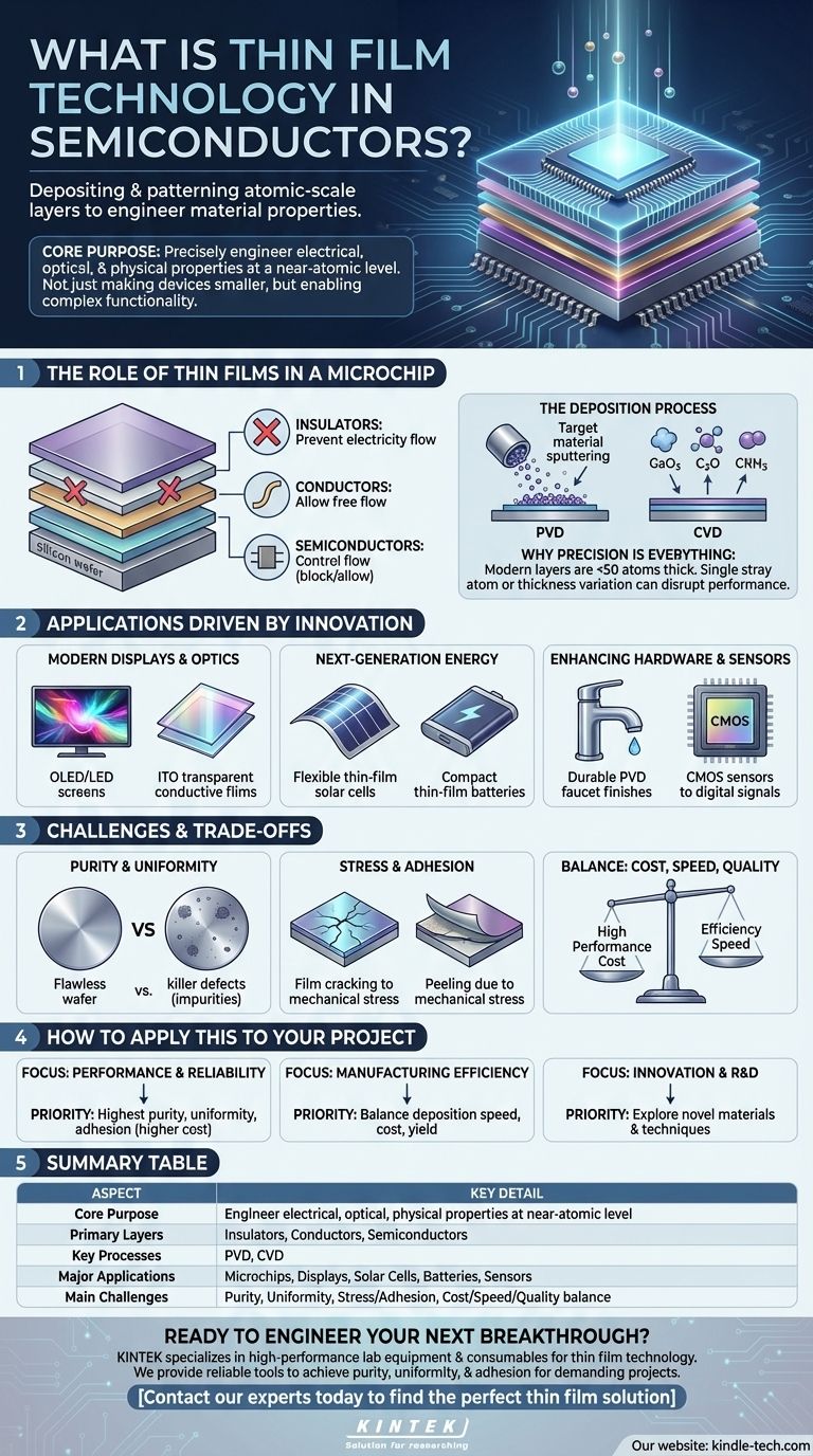
In essence, thin film technology in semiconductors is the process of depositing and patterning extremely thin layers of materials—often just a few atoms thick—onto a base material, or substrate. These layers are not merely coatings; they are the fundamental building blocks that create the intricate electrical pathways, transistors, and other components that make up a modern computer chip or electronic device.
The core purpose of thin film technology is not just to make devices smaller. It is to precisely engineer the electrical, optical, and physical properties of materials at a near-atomic level, enabling the complex functionality required by all modern electronics.
The Role of Thin Films in a Microchip
At its heart, a semiconductor device is a carefully constructed sandwich of different materials. Thin film technology is the set of techniques used to create each layer of that sandwich with incredible precision.
The Three Critical Layers
Every integrated circuit is built from three fundamental types of thin films: insulators, which prevent the flow of electricity; conductors, which allow it to flow freely; and semiconductors, which can be controlled to either block or allow flow. Together, these layers form the millions or billions of transistors on a single chip.
The Deposition Process
These films are created using processes like Physical Vapor Deposition (PVD) or Chemical Vapor Deposition (CVD). These techniques take a source material and deposit it, molecule by molecule, onto the silicon wafer (substrate) to build a new layer with specific, engineered properties.
Why Precision Is Everything
As devices shrink, the thickness of these films shrinks as well. A modern transistor gate insulator can be less than 50 atoms thick. At this scale, even a single stray atom or a slight variation in thickness can disrupt electrical performance, reduce efficiency, or cause the entire device to fail.
Applications Driven by Thin Film Innovation
While foundational to computer chips, thin film technology is the enabling force behind a vast range of other advanced products. The ability to control material properties in thin layers unlocks new possibilities across industries.
Powering Modern Displays and Optics
The vibrant colors of OLED and LED screens are produced by thin films designed to emit light. Transparent conductive films like Indium Tin Oxide (ITO) are essential for touch screens and LCDs, allowing electricity to pass through while remaining invisible to the eye.
Enabling Next-Generation Energy
Thin film solar cells are lighter and more flexible than traditional silicon panels, allowing them to be integrated into windows or curved surfaces. Similarly, thin film batteries offer higher efficiency, faster charging, and a smaller footprint, revolutionizing everything from medical implants to grid-scale energy storage.
Enhancing Hardware and Sensors
The technology extends even to everyday hardware. A durable, colored finish on a modern faucet is often a PVD thin film. The CMOS sensors in every smartphone and digital camera rely on stacked thin films to convert light into the electrical signals that form an image.
Understanding the Challenges and Trade-offs
The capabilities of thin film technology are remarkable, but they come with significant engineering challenges. Achieving perfection at the nanoscale is a constant battle.
The Demand for Purity and Uniformity
Creating a film that is perfectly even and free of contaminants across an entire 12-inch silicon wafer is incredibly difficult. Any impurity or non-uniformity can become a "killer defect" that ruins the chip. This requires ultra-clean manufacturing environments and highly controlled deposition systems.
The Problem of Stress and Adhesion
Depositing a new layer of material can create mechanical stress, much like stretching a rubber band. If the stress is too high or the film doesn't adhere properly to the layer beneath it, it can crack or peel off, destroying the device's intricate structure.
The Balance of Cost, Speed, and Quality
The highest-quality deposition methods are often the slowest and most expensive. Manufacturers must constantly balance the need for perfect films with the economic realities of mass production, making trade-offs between device performance, manufacturing speed, and overall cost.
How to Apply This to Your Project
Understanding thin film technology helps you make better decisions, whether you are designing a product, managing a manufacturing process, or investing in new technology.
- If your primary focus is device performance and reliability: You must prioritize processes that deliver the highest purity, uniformity, and film adhesion, even if it increases cost.
- If your primary focus is manufacturing efficiency and cost: Your goal is to find the optimal balance between deposition speed, material cost, and acceptable device yield.
- If your primary focus is innovation and R&D: You should explore novel materials and deposition techniques to unlock new capabilities, such as those seen in flexible electronics or transparent conductors.
Ultimately, mastering the art and science of thin films is what separates functional prototypes from world-changing products.
Summary Table:
| Aspect | Key Detail |
|---|---|
| Core Purpose | To engineer electrical, optical, and physical properties of materials at a near-atomic level. |
| Primary Layers | Insulators, Conductors, and Semiconductors. |
| Key Processes | Physical Vapor Deposition (PVD), Chemical Vapor Deposition (CVD). |
| Major Applications | Microchips, OLED/LED Displays, Thin-Film Solar Cells, Sensors, and Batteries. |
| Main Challenges | Purity, Uniformity, Stress/Adhesion, and Cost/Speed/Quality trade-offs. |
Ready to engineer your next breakthrough?
Whether you're developing advanced microchips, next-generation displays, or innovative energy solutions, the precision of your thin film deposition is critical. KINTEK specializes in high-performance lab equipment and consumables for thin film technology, serving R&D and manufacturing labs.
We provide the reliable tools and expertise you need to achieve the purity, uniformity, and adhesion required for your most demanding projects. Let's discuss how our solutions can enhance your process efficiency and device performance.
Contact our experts today to find the perfect thin film solution for your laboratory.
Visual Guide