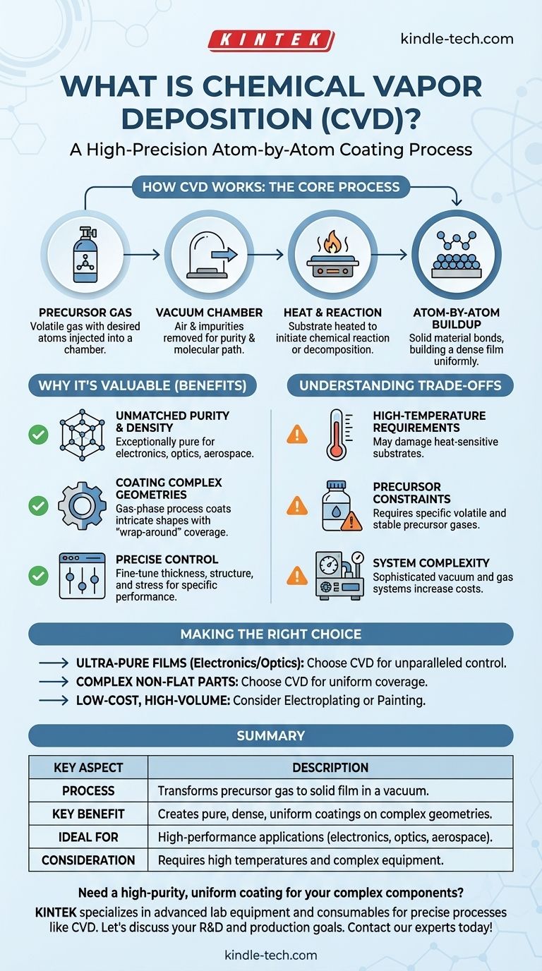
In the simplest terms, chemical vapor deposition is a high-precision process for building an ultra-thin, solid film on a surface, one atom at a time. It uses a volatile chemical gas (a "precursor") within a vacuum chamber, which reacts or decomposes when heated, depositing the desired material directly onto a component's surface to form a perfectly uniform coating.
The critical insight is that vapor deposition is not a simple spraying or dipping process. It is a sophisticated chemical construction technique that leverages a vacuum environment and controlled reactions to create highly pure, dense, and functional coatings on even the most complex shapes.
How Vapor Deposition Works: The Core Process
Vapor deposition transforms a gas into a solid film with remarkable precision. The process relies on a few fundamental components working in concert within a specialized system.
The Role of the Precursor Gas
The process begins with a precursor, a volatile chemical compound in gas form that contains the specific atoms you want to deposit. This gas is carefully injected into the process chamber.
The Importance of the Vacuum Chamber
The entire process occurs in a vacuum chamber. Removing air and other gases is crucial for two reasons: it prevents contamination of the final film and allows the precursor gas molecules to travel unimpeded to the target surface.
The Catalyst of Heat and Reaction
The component to be coated, known as the substrate, is heated to a precise reaction temperature. This heat provides the necessary energy for the precursor gas to undergo a chemical reaction or decompose when it comes into contact with the substrate's surface.
The Atom-by-Atom Buildup
As the chemical reaction occurs, the desired solid material bonds directly to the substrate's surface. Over time, this process builds up a thin, dense, and highly uniform film across the entire exposed area of the component.
Why This Method is Valuable
Chemical vapor deposition (CVD) is chosen for applications where the quality and performance of the coating are paramount. Its unique characteristics offer significant advantages over other methods.
Unmatched Purity and Density
Because the process occurs in a vacuum, the resulting film is exceptionally pure and dense. This is critical for applications in electronics, optics, and aerospace where even minuscule impurities can compromise performance.
Coating Complex Geometries
Unlike line-of-sight processes like spray painting, CVD is a gas-phase process. This means the precursor gas can reach and uniformly coat intricate, three-dimensional shapes, ensuring complete and even coverage—often called "wrap-around" properties.
Precise Control Over Film Properties
Engineers have fine-grained control over the final product. By adjusting parameters like temperature, pressure, and gas flow rates, they can precisely manipulate the coating's thickness, crystal structure, and residual stress to meet specific performance requirements.
Understanding the Trade-offs
While powerful, CVD is not a universal solution. Its precision comes with inherent complexities and limitations that must be considered.
High-Temperature Requirements
The process often relies on high temperatures to initiate the chemical reaction. This can make it unsuitable for substrates that are sensitive to heat or could be damaged by the deposition temperature.
Precursor Material Constraints
The success of CVD depends entirely on finding a suitable precursor gas. This chemical must be volatile enough to become a gas but stable enough to not decompose before reaching the substrate. Not all materials have readily available or cost-effective precursors.
System and Process Complexity
While the concept is straightforward, the equipment is not. Managing vacuum systems, handling potentially hazardous gases, and precisely controlling temperature requires sophisticated machinery and expertise, which can translate to higher operational costs.
Making the Right Choice for Your Goal
Selecting the right coating technology depends entirely on your specific objective.
- If your primary focus is creating ultra-pure, high-performance films for electronics or optics: CVD is an industry standard, offering unparalleled control over the material's purity and structure.
- If your primary focus is uniformly coating complex, non-flat parts: The exceptional "wrap-around" capability of CVD makes it a superior choice for ensuring complete and even coverage on intricate components.
- If your primary focus is low-cost, high-volume coating for non-critical applications: Simpler methods like electroplating or painting are likely more practical and economical than the precision-oriented CVD process.
Ultimately, chemical vapor deposition empowers the creation of advanced materials by providing precise control over the construction of a surface from the atoms up.
Summary Table:
| Key Aspect | Description |
|---|---|
| Process | Transforms a precursor gas into a solid film on a substrate in a vacuum chamber. |
| Key Benefit | Creates exceptionally pure, dense, and uniform coatings on complex 3D geometries. |
| Ideal For | High-performance applications in electronics, optics, and aerospace where coating quality is critical. |
| Consideration | Often requires high temperatures and sophisticated equipment, which can increase cost and complexity. |
Need a high-purity, uniform coating for your complex components?
At KINTEK, we specialize in providing advanced lab equipment and consumables for precise processes like chemical vapor deposition. Whether you are developing next-generation semiconductors, optical coatings, or aerospace components, our expertise and solutions can help you achieve the perfect film properties for your application.
Let's discuss how we can support your R&D and production goals. Contact our experts today to find the right equipment for your laboratory's needs!
Visual Guide
Related Products
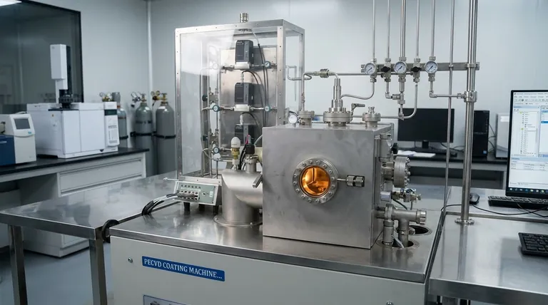
- Chemical Vapor Deposition CVD Equipment System Chamber Slide PECVD Tube Furnace with Liquid Gasifier PECVD Machine
- RF PECVD System Radio Frequency Plasma-Enhanced Chemical Vapor Deposition RF PECVD
- Microwave Plasma Chemical Vapor Deposition MPCVD Machine System Reactor for Lab and Diamond Growth
- Customer Made Versatile CVD Tube Furnace Chemical Vapor Deposition Chamber System Equipment
- 915MHz MPCVD Diamond Machine Microwave Plasma Chemical Vapor Deposition System Reactor
People Also Ask
- What are the processes of vapor phase deposition? Understand CVD vs. PVD for Superior Thin Films
- How are carbon nanotubes grown? Master Scalable Production with Chemical Vapor Deposition
- What are the core advantages of PE-CVD in OLED encapsulation? Protect Sensitive Layers with Low-Temp Film Deposition
- What types of substrates are used in CVD to facilitate graphene films? Optimize Graphene Growth with the Right Catalyst
- What is plasma enhanced chemical vapor deposition PECVD equipment? A Guide to Low-Temperature Thin Film Deposition


