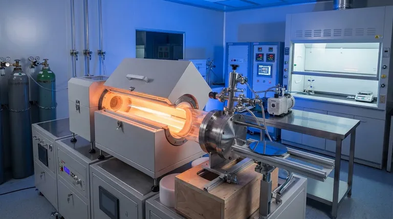
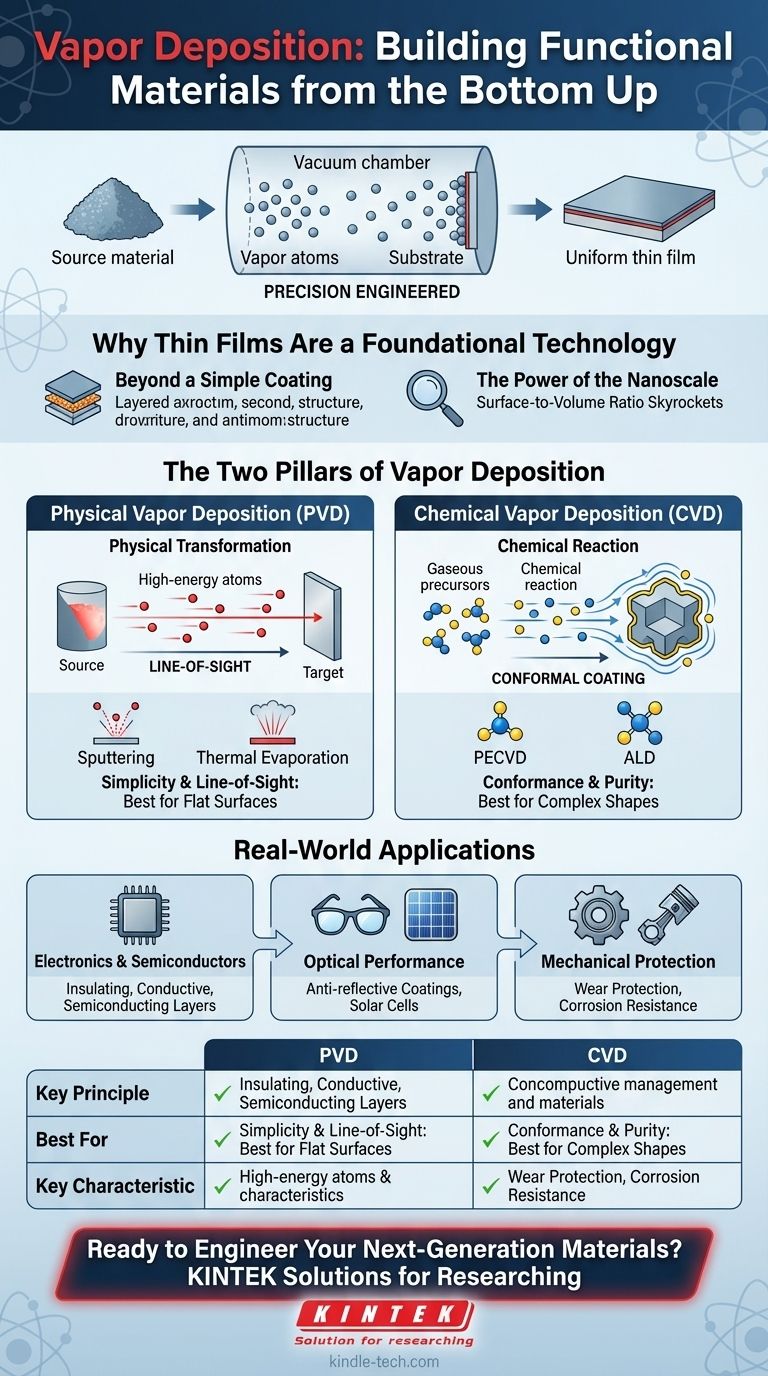
Vapor deposition is not a single process, but rather a family of advanced manufacturing techniques used to apply extremely thin layers of material onto a surface, often atom by atom. These methods involve converting a source material into a gaseous state (a vapor) and then allowing it to condense or react on a target object, known as a substrate, to form a solid film. This precise control over thickness and composition is foundational to modern technology.
At its core, vapor deposition is about building functional materials from the bottom up. By depositing materials in an atom-thin vapor form, we can engineer unique optical, electrical, and mechanical properties that are impossible to achieve in their bulk, solid-state counterparts.
Why Thin Films Are a Foundational Technology
To grasp the importance of vapor deposition, you must first understand why a thin film behaves so differently from a solid block of the same material.
Beyond a Simple Coating
A thin film is not merely a coat of paint. It is an engineered layer where the material's properties—such as its conductivity, reflectivity, or hardness—are fundamentally altered.
The Power of the Nanoscale
When materials are reduced to atomic or molecular-scale layers, their surface-to-volume ratio skyrockets. This change means that surface effects, rather than bulk properties, dominate the material's behavior, leading to the unique characteristics required for things like semiconductor devices and solar cells.
The Two Pillars of Vapor Deposition
Vapor deposition methods are broadly classified into two main categories based on how the vapor is generated and deposited. Understanding this distinction is the key to understanding the field.
Physical Vapor Deposition (PVD)
In PVD, the source material is physically transformed into a vapor. This is typically done through high-energy processes in a vacuum chamber, with no chemical reactions involved in the deposition itself.
Think of it as a form of molecular sandblasting. Atoms are knocked loose from a solid target and travel in a straight line to coat whatever is in their path. Common PVD techniques include sputtering and thermal evaporation.
Chemical Vapor Deposition (CVD)
In CVD, the film is formed from a chemical reaction on the substrate's surface. Gaseous precursor chemicals are introduced into a reaction chamber, where they decompose and react on the heated substrate to form the desired thin film.
This is more like precisely controlled condensation. The chemical precursors surround the object from all sides, allowing for a highly uniform coating. Key examples include plasma-enhanced CVD (PECVD) and atomic layer deposition (ALD).
Understanding the Trade-offs
The choice between PVD and CVD is not arbitrary; it is driven by the specific requirements of the final product. Each method comes with inherent advantages and limitations.
PVD: Simplicity and Line-of-Sight
Because the vaporized atoms in PVD travel in a straight line, it is a line-of-sight process. This makes it excellent for coating flat surfaces with high purity but less effective for covering complex, three-dimensional shapes with undercuts or hidden surfaces.
CVD: Conformance and Purity
CVD excels at creating highly conformal coatings that can uniformly cover intricate geometries. Since the deposition happens via a surface chemical reaction, the precursor gases can reach all parts of the substrate. This process can produce extremely pure and dense films.
Real-World Applications Across Industries
Vapor deposition is a hidden but essential process behind countless modern products. Its applications are defined by the specific properties being engineered into the thin film.
For Electronics and Semiconductors
Thin films are the building blocks of all integrated circuits. Vapor deposition is used to lay down the insulating, conductive, and semiconducting layers that form transistors and connectors on a silicon wafer.
For Optical Performance
Nearly every high-performance lens, from eyeglasses to scientific instruments, uses thin films. These layers are applied to create anti-reflective coatings, high-reflectivity mirrors, and filters that manipulate light. This technology is also critical for manufacturing solar cells.
For Mechanical Protection
Vapor-deposited films can create surfaces that are far more durable than the underlying material. These films provide wear protection on machine tools and engine parts, create thermal barriers in aerospace, and deliver corrosion resistance for sensitive components.
Making the Right Choice for Your Goal
The right deposition method depends entirely on the material, the shape of the substrate, and the functional goal of the final product.
- If your primary focus is creating integrated circuits or semiconductor devices: You will rely on both PVD and CVD for depositing the various conductive, insulating, and semiconducting layers with extreme precision.
- If your primary focus is enhancing optical properties: PVD is often the standard for creating anti-reflective lens coatings, while CVD and its variants are crucial for manufacturing high-purity optical waveguides.
- If your primary focus is improving durability and corrosion resistance: PVD is excellent for applying hard, wear-resistant coatings to tools, while CVD can create highly conformal protective layers for complex industrial components.
Ultimately, understanding vapor deposition is key to unlocking the material properties that define modern technology.
Summary Table:
| Method | Key Principle | Best For | Key Characteristic |
|---|---|---|---|
| Physical Vapor Deposition (PVD) | Physical transformation of a solid into a vapor. | Flat surfaces, high-purity coatings, wear protection. | Line-of-sight process. |
| Chemical Vapor Deposition (CVD) | Chemical reaction of gases on a heated substrate. | Complex 3D shapes, highly uniform and conformal coatings. | Excellent step coverage. |
Ready to Engineer Your Next-Generation Materials?
Whether you're developing advanced semiconductors, optical coatings, or wear-resistant components, the right deposition equipment is critical to your success. KINTEK specializes in high-quality lab equipment and consumables for all your vapor deposition needs.
We provide the tools and expertise to help you:
- Achieve precise, uniform thin films for R&D and production.
- Select the optimal PVD or CVD system for your specific application.
- Enhance the performance and durability of your products.
Let's discuss how our solutions can accelerate your innovation. Contact our experts today for a personalized consultation!
Visual Guide
Related Products
- Chemical Vapor Deposition CVD Equipment System Chamber Slide PECVD Tube Furnace with Liquid Gasifier PECVD Machine
- RF PECVD System Radio Frequency Plasma-Enhanced Chemical Vapor Deposition RF PECVD
- 915MHz MPCVD Diamond Machine Microwave Plasma Chemical Vapor Deposition System Reactor
- Microwave Plasma Chemical Vapor Deposition MPCVD Machine System Reactor for Lab and Diamond Growth
- HFCVD Machine System Equipment for Drawing Die Nano-Diamond Coating
People Also Ask
- What is plasma enhanced chemical vapor deposition PECVD equipment? A Guide to Low-Temperature Thin Film Deposition
- How expensive is chemical vapor deposition? Understanding the True Cost of High-Performance Coating
- What types of substrates are used in CVD to facilitate graphene films? Optimize Graphene Growth with the Right Catalyst
- How are carbon nanotubes grown? Master Scalable Production with Chemical Vapor Deposition
- What happens during deposition chemistry? Building Thin Films from Gaseous Precursors


