In essence, Chemical Vapor Deposition (CVD) is a highly versatile manufacturing process used to create thin, solid films on a surface (a substrate) from gaseous chemical precursors. The core principle involves flowing one or more reactive gases into a chamber where they decompose and react on or near a heated substrate, depositing a layer of material. The many "types" of CVD are simply variations on this theme, each optimized for specific materials, temperatures, or desired film properties.
The array of CVD acronyms—LPCVD, PECVD, MOCVD—can be confusing. The key is to understand they are not entirely different processes, but rather modifications of a core technique. Each variant controls a specific variable—primarily pressure, temperature, or the energy source—to solve a particular engineering problem.
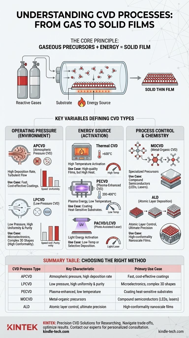
The Core Principle of CVD
From Gas to Solid Film
At its heart, every CVD process involves a chemical reaction. Gaseous molecules, known as precursors, are introduced into a reaction chamber containing the object to be coated, called the substrate.
Energy is applied to the system, typically as heat. This energy causes the precursor gases to react and/or decompose, forming a stable solid material that deposits onto the substrate, creating a thin, uniform film.
Think of it like frost forming on a cold window pane. Water vapor (the precursor gas) in the air comes into contact with the cold glass (the substrate) and, under the right conditions, changes from a gas into a solid layer of ice (the film). CVD is a more complex version involving controlled chemical reactions.
The Key Variables That Define CVD Processes
The specific "type" of CVD is determined by how it manipulates a few fundamental parameters. Understanding these variables provides a framework for navigating the different techniques.
Operating Pressure (The Environment)
Pressure inside the reaction chamber dictates how gas molecules travel and interact.
- Atmospheric Pressure CVD (APCVD): As the name implies, this process runs at normal atmospheric pressure. It allows for very high deposition rates, making it fast and relatively inexpensive. However, gas flow can be turbulent, sometimes leading to lower film uniformity and purity.
- Low-Pressure CVD (LPCVD): This process operates in a partial vacuum. The lower pressure allows gas molecules to move more freely, resulting in highly uniform and pure films that can coat even complex, three-dimensional shapes with exceptional consistency (known as high conformality).
Energy Source (The Activation Method)
Energy is required to initiate the chemical reaction. The source of this energy is a major differentiator.
- Thermal CVD: This is the most fundamental form, relying solely on high temperatures (often >600°C) to provide the activation energy. While it produces high-quality films, its high heat makes it unsuitable for coating materials with low melting points, like plastics or certain metal alloys.
- Plasma-Enhanced CVD (PECVD): This technique uses an electric field to generate a plasma (an ionized gas) within the chamber. The energetic plasma provides the energy to drive the reaction, allowing deposition to occur at much lower temperatures (typically 200-400°C). This is critical for coating heat-sensitive substrates.
- Photo-Assisted CVD (PACVD or LCVD): In this variant, light—often from a UV lamp or a laser—is used to supply the reaction energy. This can be used for low-temperature deposition or to selectively deposit material only where the light is aimed.
Precursor Chemistry (The Building Blocks)
Sometimes, the type of chemical used as the precursor defines the process.
- Metal-Organic CVD (MOCVD): This is a specialized form of thermal CVD that uses metal-organic compounds as precursors. It is the dominant technology for manufacturing high-performance compound semiconductors used in LEDs, lasers, and high-frequency electronics.
Process Control (The Ultimate Precision)
One variant of CVD takes process control to the extreme.
- Atomic Layer Deposition (ALD): Often considered a subtype of CVD, ALD is a sequential process. It introduces precursors one at a time, allowing them to form a single, self-limiting atomic layer before the next precursor is introduced. This builds the film one atomic layer at a time, providing unparalleled control over thickness and perfect conformality on the most complex structures.
Understanding the Trade-offs
Choosing a CVD method involves balancing competing factors. There is no single "best" process; there is only the best process for a specific application.
Temperature vs. Substrate Compatibility
High-temperature thermal CVD can produce exceptionally pure, crystalline films. However, these temperatures will damage or destroy many substrates, such as tempered steel tools, aluminum, or polymers. PECVD is the direct solution to this, but the resulting films may have different properties (e.g., higher internal stress or hydrogen incorporation) than their high-temperature counterparts.
Deposition Rate vs. Film Quality
Faster deposition is better for manufacturing throughput. APCVD is very fast but can struggle to produce the defect-free, uniform films required for microelectronics. Slower processes like LPCVD and especially ALD offer superior quality and control but at the cost of significantly longer process times.
Conformality vs. Simplicity
A major strength of CVD, particularly LPCVD and ALD, is its ability to uniformly coat deep trenches and internal surfaces. This is a significant advantage over line-of-sight processes like physical vapor deposition (PVD). However, achieving this requires complex vacuum systems and precise process control, making the equipment more expensive and challenging to operate.
Making the Right Choice for Your Goal
To select the appropriate method, you must first define your most critical requirement.
- If your primary focus is high-throughput, low-cost coatings: APCVD is often the most economical choice for applications where perfect uniformity is not critical.
- If your primary focus is high purity and uniformity on complex shapes: LPCVD is the workhorse for many microelectronics and materials science applications.
- If your primary focus is coating temperature-sensitive materials: PECVD is the necessary solution to avoid thermal damage to the substrate.
- If your primary focus is ultimate precision and atomic-level control: ALD is the only method that provides angstrom-level thickness control and perfect conformality.
By understanding how each process manipulates these core variables, you can confidently select the right tool for any material deposition challenge.
Summary Table:
| CVD Process Type | Key Characteristic | Primary Use Case |
|---|---|---|
| APCVD | Atmospheric pressure, high deposition rate | Fast, cost-effective coatings |
| LPCVD | Low pressure, high uniformity & purity | Microelectronics, complex 3D shapes |
| PECVD | Plasma-enhanced, low temperature | Coating heat-sensitive substrates |
| MOCVD | Metal-organic precursors | Compound semiconductors (LEDs, lasers) |
| ALD | Atomic layer control, ultimate precision | High-conformality nanoscale films |
Struggling to select the right CVD process for your specific substrate and performance requirements? KINTEK specializes in lab equipment and consumables, serving laboratory needs with precision CVD solutions. Our experts can help you navigate the trade-offs between temperature, deposition rate, and film quality to achieve optimal results for your application. Contact our team today for a personalized consultation and discover how our CVD expertise can enhance your research and development.
Visual Guide
Related Products
- Customer Made Versatile CVD Tube Furnace Chemical Vapor Deposition Chamber System Equipment
- Chemical Vapor Deposition CVD Equipment System Chamber Slide PECVD Tube Furnace with Liquid Gasifier PECVD Machine
- CVD Diamond for Thermal Management Applications
- Custom CVD Diamond Coating for Lab Applications
- HFCVD Machine System Equipment for Drawing Die Nano-Diamond Coating
People Also Ask
- How does a CVD tube furnace inhibit the sintering of silver supports? Boost Membrane Durability and Performance
- What is the effect of temperature on graphene oxide? Master Thermal Reduction for Precise Material Properties
- What is the function of a tube furnace in CVD SiC synthesis? Achieving Ultra-Pure Silicon Carbide Powders
- What is the difference between hot wall CVD and cold wall CVD? Choose the Right System for Your Process
- What is the application of CVD in nanotechnology? Harness Atomic-Level Precision for Next-Gen Materials


