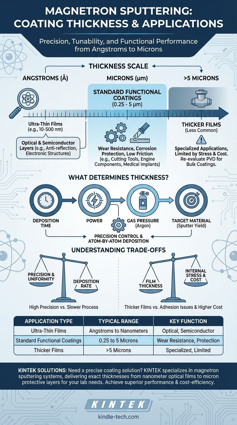
For magnetron sputtering, the typical coating thickness ranges from a few angstroms (Å) for highly specialized applications to several microns (µm) for functional surfaces. Most common industrial applications, such as for wear resistance or corrosion protection, produce coatings between 0.25 and 5 microns.
The essential takeaway is not a single thickness value, but the process's exceptional control. Magnetron sputtering allows for the precise, atom-by-atom deposition of films, enabling engineers to tailor a coating's thickness to its exact functional requirement, whether for optical performance or mechanical durability.
What Determines Coating Thickness?
The final thickness of a sputtered film is not an inherent property but a direct result of several controllable process parameters. Understanding these factors is key to achieving a consistent and effective coating.
The Sputtering Process in Brief
Magnetron sputtering is a Physical Vapor Deposition (PVD) process. It begins by creating a plasma—an ionized gas, typically Argon—in a vacuum chamber. A strong magnetic field traps electrons near the surface of the source material (the "target"), which dramatically increases the efficiency of ion formation. These positive ions are then accelerated into the negatively charged target, striking it with enough force to physically knock atoms loose. These ejected atoms travel through the chamber and deposit onto your component, building the coating one atomic layer at a time.
Key Control Parameters
The thickness is primarily governed by a few variables:
- Deposition Time: The longer the substrate is exposed to the flux of sputtered atoms, the thicker the coating will be.
- Power: Increasing the electrical power applied to the target increases the rate of ion bombardment, which in turn increases the rate at which atoms are sputtered and deposited.
- Gas Pressure: The pressure of the argon gas inside the chamber affects the density of the plasma and the energy of the ions, influencing the sputtering rate.
- Target Material: Different materials have different "sputter yields"—the number of atoms ejected per incoming ion. Materials with higher yields will build a coating faster than those with lower yields.
Functional Thickness: From Angstroms to Microns
The required thickness is dictated entirely by the coating's intended purpose. Different applications operate on vastly different scales.
Ultra-Thin Films (Angstroms to Nanometers)
In this range (1 nanometer = 10 angstroms), coatings are used for their optical or electrical properties. A layer just a few hundred angstroms thick can create an anti-reflection surface on a lens by causing destructive light wave interference. In semiconductors, layers of this scale are used to build up complex electronic structures.
Standard Functional Coatings (0.25 to 5 Microns)
This is the most common range for mechanical applications. A coating of 1 to 4 microns of a material like Titanium Nitride (TiN) or Diamond-Like Carbon (DLC) provides a significant increase in surface hardness, wear resistance, and a low coefficient of friction. This is ideal for cutting tools, engine components, and medical implants.
Thicker Films (Above 5 Microns)
While possible, creating very thick films with sputtering becomes progressively more challenging and costly. The primary reason is not the process itself, but the physics of the deposited film.
Understanding the Trade-offs
Choosing a coating thickness is an engineering decision that involves balancing performance goals with practical limitations.
Precision vs. Deposition Rate
Sputtering offers unparalleled precision and uniformity, but it is not the fastest deposition method. Building up a very thick coating (e.g., 20+ microns) can be time-consuming and, therefore, expensive compared to processes like thermal spray or electroplating.
Internal Stress and Adhesion
As a film gets thicker, internal stresses from the deposition process can accumulate. If this stress becomes too high, it can exceed the coating's adhesion strength to the substrate, leading to cracking, flaking, or delamination. This is a critical limiting factor for thick sputtered coatings.
Cost and Throughput
Longer deposition times directly translate to higher costs due to increased machine time, energy consumption, and gas usage. For many applications, the performance benefit of adding another micron of thickness is not worth the associated increase in cost and process time.
Selecting the Right Thickness for Your Application
Use your end goal to guide your specification.
- If your primary focus is optical properties or semiconductors: You will likely operate in the nanometer range (10-500 nm) for precise light interference or electrical function.
- If your primary focus is wear resistance or corrosion protection: Target the standard industrial range of 0.5 to 5 microns to achieve a durable, hard-wearing surface without introducing excessive internal stress.
- If you need a very thick coating (over 10 microns): Re-evaluate if magnetron sputtering is the most cost-effective method; other deposition technologies may be better suited for bulk coatings.
Ultimately, magnetron sputtering's strength lies in its tunability, allowing you to engineer a coating thickness that precisely matches your component's functional demands.
Summary Table:
| Application Type | Typical Thickness Range | Key Function |
|---|---|---|
| Ultra-Thin Films | Angstroms to Nanometers (e.g., 10-500 nm) | Optical coatings, semiconductor layers |
| Standard Functional Coatings | 0.25 to 5 Microns | Wear resistance, corrosion protection, low friction |
| Thicker Films | > 5 Microns (Less Common) | Specialized applications, limited by stress and cost |
Need a precise coating solution for your lab equipment? KINTEK specializes in magnetron sputtering systems and consumables, delivering the exact coating thickness your application demands—from nanometer-scale optical films to micron-thick protective layers. Achieve superior performance, durability, and cost-efficiency for your laboratory needs. Contact our experts today to discuss your project!
Visual Guide
Related Products
- Electron Beam Evaporation Coating Oxygen-Free Copper Crucible and Evaporation Boat
- Custom PTFE Teflon Parts Manufacturer for Magnetic Stirring Bar
- Infrared Transmission Coating Sapphire Sheet Substrate Window
- 400-700nm Wavelength Anti Reflective AR Coating Glass
- Custom CVD Diamond Coating for Lab Applications
People Also Ask
- What is e-beam evaporation? Achieve High-Purity Thin Film Deposition for Your Lab
- What are the applications of e-beam evaporation? Achieve High-Purity Coatings for Optics & Electronics
- What is the container that holds the metal source material called in e-beam evaporation? Ensure Purity and Quality in Your Thin-Film Deposition
- What is the temperature of e-beam evaporation? Mastering the Two-Zone Thermal Process for Precision Films
- What are the applications of electron beams? From Nanoscale Imaging to Industrial Manufacturing


