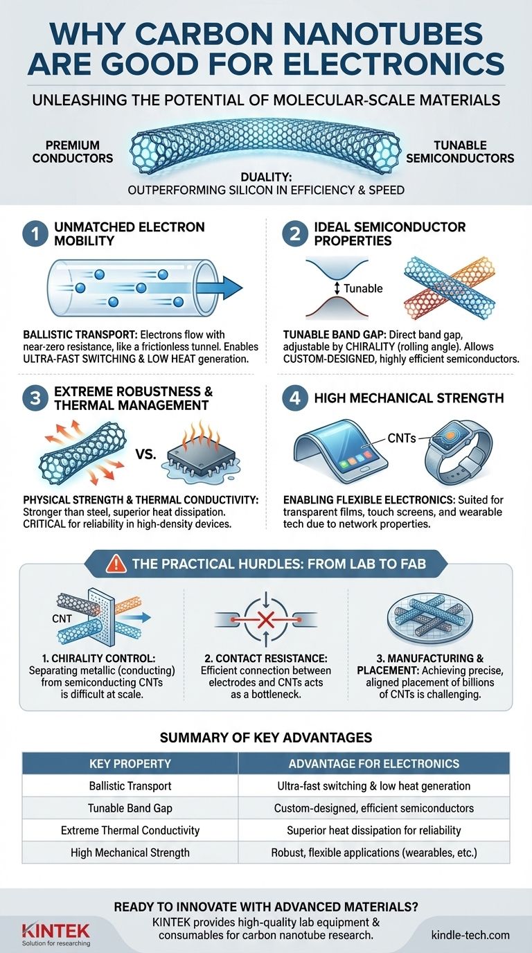
At their core, carbon nanotubes (CNTs) are exceptional for electronics because they combine the high-speed electrical performance of premium conductors with the tunable, switchable properties of semiconductors in a single, molecular-scale material. This unique duality allows them to potentially outperform silicon in creating smaller, faster, and more energy-efficient electronic components.
The true promise of carbon nanotubes isn't just that they are better than existing materials in one area; it's their potential to create an entirely new class of electronics that are fundamentally more efficient and powerful, operating closer to the physical limits of computation.

Why CNTs Challenge Silicon's Dominance
For decades, silicon has been the undisputed foundation of the electronics industry. However, as transistors shrink to near-atomic sizes, silicon is approaching its physical limits, facing challenges with heat generation and quantum effects. CNTs offer a path forward.
Unmatched Electron Mobility
Electrons move through certain types of carbon nanotubes with almost no resistance, a phenomenon known as ballistic transport. Imagine electrons flowing through a wire like cars in heavy traffic, constantly bumping into things and losing energy. In a CNT, it's like an empty, frictionless tunnel.
This property means CNT-based transistors can switch on and off much faster while generating significantly less heat. This directly translates to higher processing speeds and better energy efficiency in devices.
Ideal Semiconductor Properties
A material's usefulness as a semiconductor is defined by its band gap—an energy barrier that determines how easily it can switch between an "on" (conducting) and "off" (insulating) state. CNTs have a direct band gap, which is highly efficient for this switching.
More importantly, the band gap of a CNT can be precisely controlled based on its chirality, which is the angle at which the original graphene sheet is "rolled" to form the tube. This opens the door to custom-designing semiconductors for specific applications, something not possible with silicon.
Extreme Physical and Thermal Robustness
CNTs are one of the strongest materials ever discovered, possessing incredible tensile strength and stiffness. They are also excellent thermal conductors, able to dissipate heat far more effectively than copper or silicon.
In an electronic device, where billions of transistors generate immense heat in a tiny space, this ability to manage heat is critical for reliability and performance.
The Practical Hurdles: From Lab to Fab
While the theoretical advantages of CNTs are immense, translating them from laboratory experiments to mass-produced consumer electronics ("fab") presents significant engineering challenges.
The Chirality Control Problem
CNTs can be either metallic (always conducting, like a wire) or semiconducting, depending on their chirality. A batch of synthesized CNTs almost always contains a random mix of both types.
For building transistors, you need purely semiconducting CNTs. Even a single metallic CNT in the wrong place can create a short circuit, rendering the transistor useless. Separating these types with near-100% purity at an industrial scale remains a major obstacle.
The Contact Resistance Problem
Efficiently getting electricity into and out of a molecule-sized nanotube is not trivial. The connection point, or contact, between the metal electrode and the CNT can create significant electrical resistance.
This resistance acts as a bottleneck, negating the benefits of the CNT's high-speed internal transport. Overcoming this contact resistance is a primary focus of current research.
The Manufacturing and Placement Problem
Silicon manufacturing is a mature, ultra-precise process. We can place billions of identical silicon transistors exactly where we want them. Replicating this precision with CNTs is extraordinarily difficult.
Developing methods to grow or deposit vast arrays of perfectly aligned, uniformly structured CNTs on a wafer is the key to unlocking their potential for complex integrated circuits like CPUs.
Making the Right Choice for Your Goal
Understanding the specific application is key to evaluating the viability of carbon nanotubes. Their current strengths are best suited for particular domains where their unique properties outweigh the manufacturing challenges.
- If your primary focus is next-generation processors: The goal is replacing silicon channels in transistors (CNTFETs) to achieve higher speeds and efficiency, but this faces the most significant chirality and placement hurdles.
- If your primary focus is flexible or transparent electronics: CNTs are a leading candidate for creating transparent conductive films for touch screens and flexible displays, as their network properties are more forgiving than the purity required for transistors.
- If your primary focus is high-frequency communication: The exceptional carrier mobility in CNTs makes them ideal for radio frequency (RF) devices that operate at speeds far beyond the capability of silicon.
- If your primary focus is advanced sensors: The high surface-area-to-volume ratio of CNTs makes them extremely sensitive to their chemical environment, enabling the creation of highly specific and responsive molecular sensors.
Ultimately, carbon nanotubes represent a fundamental shift in how we can build electronic devices from the molecule up.
Summary Table:
| Key Property | Advantage for Electronics |
|---|---|
| Ballistic Transport | Electrons flow with near-zero resistance, enabling ultra-fast switching and low heat generation. |
| Tunable Band Gap | Direct, chirality-dependent band gap allows for custom-designed, highly efficient semiconductors. |
| Extreme Thermal Conductivity | Superior heat dissipation improves device reliability and performance at high densities. |
| High Mechanical Strength | Enables robust, flexible electronic applications like wearable tech and transparent displays. |
Ready to explore how advanced materials can power your next innovation?
KINTEK specializes in providing the high-quality lab equipment and consumables needed for cutting-edge materials research, including the development of carbon nanotube-based electronics. Our products support the precise synthesis and analysis required to overcome the challenges of chirality control and manufacturing.
Contact our experts today to discuss how we can support your laboratory's specific needs and help you push the boundaries of electronic performance.
Visual Guide
Related Products
- Carbon Graphite Boat -Laboratory Tube Furnace with Cover
- Boron Nitride (BN) Ceramic Tube
- Hexagonal Boron Nitride HBN Thermocouple Protection Tube
People Also Ask
- What is the disadvantage of graphite furnace? Managing Reactivity and Contamination Risks
- Why graphite is used as a crucible to melt metal? Unlock Superior High-Temperature Performance
- Why is graphite used in furnaces? For Extreme Heat, Purity, and Efficiency
- What is the use of graphite tube? Essential for Extreme Heat & Corrosive Environments
- Why is a graphite crucible containing molten bismuth used in LiF–NaF–KF purification? Enhance Melt Purity Efficiently