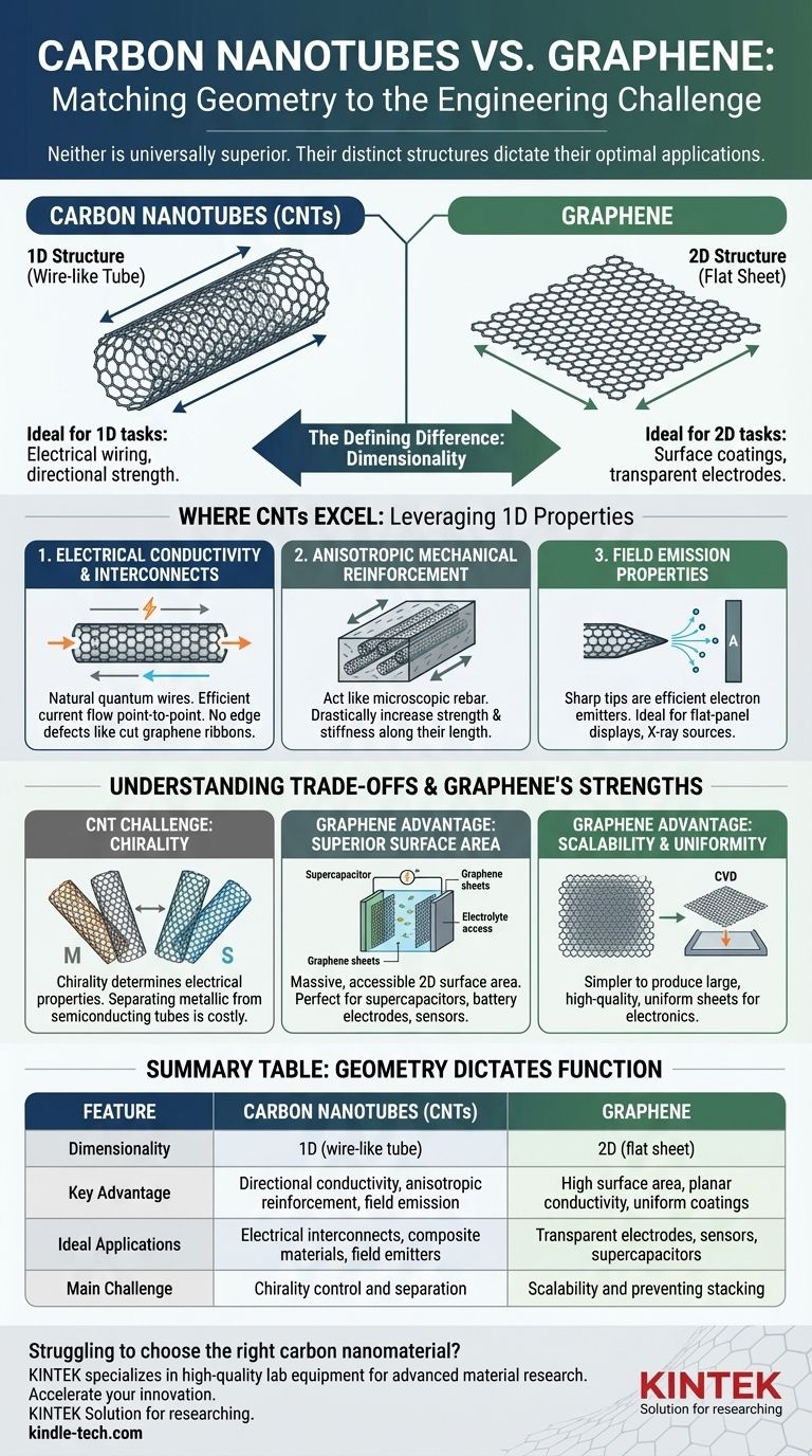
The question of whether carbon nanotubes are "better" than graphene is a common point of confusion, and the answer is not a simple "yes." Neither material is universally superior. Instead, their distinct atomic structures—one being a rolled-up tube and the other a flat sheet—give them fundamentally different advantages. Carbon nanotubes (CNTs) excel in applications requiring one-dimensional properties, like electrical wiring, while graphene's two-dimensional nature makes it ideal for applications like surface coatings or transparent electrodes.
Choosing between carbon nanotubes and graphene is not about determining a "winner," but about matching material geometry to the engineering challenge. CNTs are superior for tasks that leverage their one-dimensional (1D) structure, while graphene excels at tasks that require its two-dimensional (2D) properties.
The Defining Difference: Dimensionality and Structure
To understand their uses, you must first appreciate their fundamental geometric difference. Both are allotropes of carbon, but their shapes dictate their function.
Graphene: The Quintessential 2D Material
Graphene is a single, flat sheet of carbon atoms arranged in a honeycomb lattice. It is, for all practical purposes, a two-dimensional material.
This structure gives it an extremely high surface-area-to-volume ratio. Think of it as a perfect, atom-thin plane, making every atom available for interaction on its surface.
Carbon Nanotubes: A Rolled-Up Dimension
A carbon nanotube is essentially a sheet of graphene that has been seamlessly rolled into a cylindrical tube. This act of "rolling" transforms the material from 2D to 1D.
This tubular structure confines electrons, forcing them to primarily travel along the length of the tube, much like water flowing through a pipe. This has profound implications for its electrical and mechanical properties.
Where Carbon Nanotubes Have a Distinct Advantage
The framing of your question points to a desire to know the specific scenarios where a CNT is the superior choice. These are primarily applications that benefit from its wire-like, 1D nature.
Electrical Conductivity and Interconnects
For moving electrical current from point A to point B, CNTs are naturally suited for the job. Their structure acts as a perfect quantum wire.
While graphene is an excellent conductor, its 2D nature means current flows across a plane. To create a "wire" from graphene, it must be patterned and cut into a narrow ribbon, which can introduce edge defects and complicate manufacturing. A CNT is already a wire by its very nature.
Anisotropic Mechanical Reinforcement
The exceptional tensile strength and high aspect ratio (length vs. diameter) of CNTs make them ideal for reinforcing composites.
When aligned within a polymer matrix, they act like microscopic rebar, drastically increasing strength and stiffness along their length. This is an anisotropic effect—the strength is directional. Graphene adds planar, or isotropic, strength but can be more prone to stacking and clumping within a matrix.
Field Emission Properties
The sharp, curved tips of carbon nanotubes are incredibly efficient at emitting electrons under an electric field. This is a property known as field emission.
This makes CNTs highly valuable for applications like flat-panel displays (field emission displays), novel X-ray sources, and vacuum electronics. Graphene's flat surface does not possess these ideal emission points.
Understanding the Trade-offs
A balanced analysis requires acknowledging where CNTs fall short. Choosing them blindly can lead to significant engineering challenges.
The Challenge of Chirality
The specific angle at which the graphene sheet is "rolled" to form a nanotube is called its chirality. This single detail determines if the CNT behaves like a metal or a semiconductor.
Synthesizing CNTs produces a mixture of different chiralities. Separating the metallic from the semiconducting tubes is a major, expensive hurdle for creating reliable electronics, a problem graphene does not have.
Graphene's Superior Surface Area
For applications that depend on a massive, accessible surface area—such as supercapacitors, battery electrodes, and chemical sensors—graphene is the clear winner.
Its open, 2D planar structure ensures that reactants and electrolytes can access the entire surface. The walls of a nanotube are less accessible, especially in multi-walled structures.
Scalability and Uniformity
Manufacturing processes like Chemical Vapor Deposition (CVD) have enabled the production of very large, high-quality, single-layer graphene sheets with high uniformity.
While CNT production has advanced, achieving precise control over length, diameter, and especially chirality at an industrial scale remains a more significant challenge. This makes graphene a more predictable material for certain large-area applications.
Making the Right Choice for Your Application
Your material selection must be driven by the specific problem you are trying to solve.
- If your primary focus is creating nano-scale wiring, directional composites, or field emitters: The inherent 1D geometry and high aspect ratio of CNTs make them the superior choice.
- If your primary focus is developing transparent conductive films, high-surface-area sensors, or impermeable coatings: Graphene's 2D structure, large surface area, and planar nature make it the more suitable material.
- If your primary focus is scalable, predictable semiconductor electronics: Graphene is often simpler to integrate, as you avoid the costly problem of separating mixed-chirality CNTs.
Ultimately, the power of these materials is unlocked not by pitting them against each other, but by correctly applying their unique geometries to solve specific engineering challenges.
Summary Table:
| Feature | Carbon Nanotubes (CNTs) | Graphene |
|---|---|---|
| Dimensionality | 1D (wire-like tube) | 2D (flat sheet) |
| Key Advantage | Directional conductivity, anisotropic reinforcement, field emission | High surface area, planar conductivity, uniform coatings |
| Ideal Applications | Electrical interconnects, composite materials, field emitters | Transparent electrodes, sensors, supercapacitors |
| Main Challenge | Chirality control and separation | Scalability and preventing stacking |
Struggling to choose the right carbon nanomaterial for your lab's specific application? KINTEK specializes in providing high-quality lab equipment and consumables tailored to advanced material research. Whether you're developing next-generation electronics with carbon nanotubes or creating high-surface-area sensors with graphene, our expertise ensures you have the right tools for precision and scalability. Contact our experts today to discuss how we can support your laboratory's unique needs and accelerate your innovation.
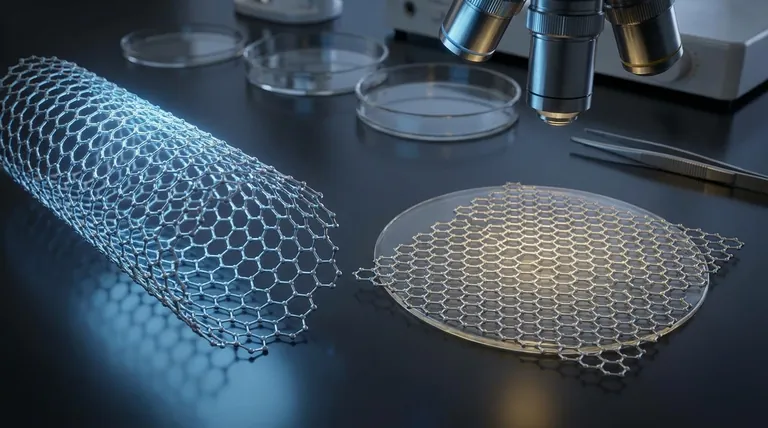
Visual Guide