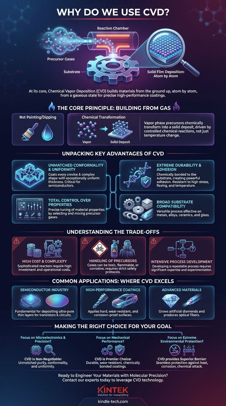
At its core, Chemical Vapor Deposition (CVD) is used because it provides an exceptionally precise way to create high-performance thin films and coatings on a substrate. The process allows for the construction of materials, atom by atom, from a gaseous state. This results in coatings that are incredibly pure, uniform, durable, and can be applied to even the most complex and intricate surfaces.
The true power of CVD is its ability to build materials from the ground up using chemical reactions. This fundamental difference from physical coating methods gives engineers unparalleled control over a material's final properties, from its wear resistance to its electrical conductivity.
The Core Principle: Building Materials from Gas
Chemical Vapor Deposition is not like painting or dipping an object. Instead of applying a pre-made liquid or powder, CVD introduces precursor gases into a reaction chamber containing the object (substrate) you wish to coat.
A Chemical Transformation
These gases react or decompose on the hot surface of the substrate, leaving behind a solid material. The "vapor" phase precursors chemically transform into a solid "deposit."
This process is more like frost forming on a cold window—a gas (water vapor) turns directly into a solid (ice)—but it is driven by controlled chemical reactions rather than just temperature change. This atomic-level deposition is the source of all of CVD's major advantages.
Unpacking the Key Advantages of CVD
The reason CVD is so prevalent in high-tech industries stems from a few key capabilities that are difficult or impossible to achieve with other methods.
Unmatched Conformality and Uniformity
Because the precursor gas can flow into every crevice of a substrate, the resulting solid film is perfectly conformal. It coats internal channels, sharp corners, and complex 3D shapes with a layer of exceptionally uniform thickness.
This is absolutely critical in the semiconductor industry, where microscopic electronic components require perfectly even layers to function correctly.
Extreme Durability and Adhesion
A CVD coating isn't just "stuck on" the surface; it is chemically bonded to it. This creates a powerful bond between the coating and the substrate.
As a result, CVD coatings are highly durable and remain intact even in high-stress environments involving flexing, bending, or extreme temperature variations.
Total Control Over Material Properties
By carefully selecting and mixing the precursor gases, engineers can tune the exact properties of the final deposited material.
This allows for the creation of films optimized for specific functions, such as:
- Wear Resistance: For cutting tools and engine parts.
- Corrosion Resistance: For components in harsh chemical environments.
- High Lubricity: Creating low-friction surfaces.
- High Purity: Essential for semiconductors and optical fibers.
- Chemical Inertness: For medical implants and protective barriers.
Broad Substrate Compatibility
CVD is a highly versatile process that is not limited to one type of base material. It is routinely used to coat a wide variety of substrates, including metals, specialized alloys, ceramics, and even glass.
Understanding the Trade-offs
No process is perfect, and choosing CVD means accepting certain complexities. Understanding these trade-offs is key to making an informed decision.
High Initial Cost and Complexity
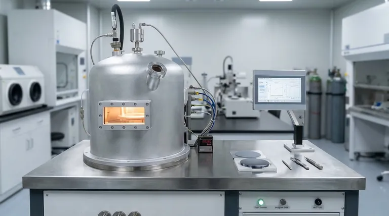
CVD reactors are sophisticated pieces of equipment that require high temperatures, vacuum systems, and precise gas control. This makes the initial investment and operational costs higher than simpler coating methods like electroplating or painting.
Handling of Precursor Materials
The precursor gases used in CVD can be toxic, flammable, or corrosive. The process requires stringent safety protocols and specialized handling infrastructure, which adds to the overall complexity and cost.
Process Development Can Be Intensive
CVD is not a "one-size-fits-all" solution. Developing a stable and repeatable process for a new application requires significant expertise and experimentation to optimize the temperature, pressure, gas flow rates, and chemistry.
Common Applications: Where CVD Excels
CVD's unique benefits make it the go-to process in several demanding fields.
In the Semiconductor Industry
CVD is fundamental to modern electronics. It is used to deposit the ultra-pure, uniform, and thin layers of silicon, silicon dioxide, and other materials that form the transistors and circuits inside microchips.
For High-Performance Coatings
The process is used to apply hard coatings to machine tools, increasing their lifespan and performance. It also creates wear-resistant surfaces on automotive parts and corrosion-proof barriers on chemical processing equipment.
In Advanced Materials
CVD's versatility extends beyond simple coatings. It is one of the primary methods used to grow high-purity artificial diamonds for industrial and electronic applications, as well as the core material for optical fibers used in global telecommunications.
Making the Right Choice for Your Goal
When deciding if CVD is the right process, consider the primary engineering problem you are trying to solve.
- If your primary focus is microelectronics and precision: CVD is often non-negotiable due to its unmatched ability to create pure, conformal, and uniform thin films at a microscopic scale.
- If your primary focus is enhancing mechanical performance: CVD is the premier choice for creating durable, wear-resistant, or low-friction coatings that are chemically bonded to tools and components.
- If your primary focus is extreme environmental protection: CVD provides a superior, seamless barrier against high temperatures, corrosion, and chemical attack.
Ultimately, CVD is the process of choice when you need to engineer a material's surface with molecular-level precision.
Summary Table:
| Key Advantage | Why It Matters |
|---|---|
| Conformal & Uniform Coating | Ensures even coverage on complex 3D shapes and microscopic features. |
| Exceptional Durability & Adhesion | Creates a strong chemical bond for coatings that last in high-stress environments. |
| Tailored Material Properties | Allows precise control over characteristics like wear resistance and conductivity. |
| Broad Substrate Compatibility | Effective on a wide range of materials including metals, ceramics, and glass. |
Ready to Engineer Your Materials with Molecular Precision?
If your project demands ultra-pure, uniform, and durable thin films, the advanced capabilities of Chemical Vapor Deposition (CVD) are essential. KINTEK specializes in providing the high-performance lab equipment and expert support needed to leverage CVD technology for your most challenging applications, from semiconductor manufacturing to creating wear-resistant coatings.
Contact our experts today to discuss how our solutions can help you achieve superior results.
Visual Guide
Related Products
- CVD Diamond Dressing Tools for Precision Applications
- CVD Diamond Domes for Industrial and Scientific Applications
- Multi Heating Zones CVD Tube Furnace Machine Chemical Vapor Deposition Chamber System Equipment
- CVD Diamond for Thermal Management Applications
- Chemical Vapor Deposition CVD Equipment System Chamber Slide PECVD Tube Furnace with Liquid Gasifier PECVD Machine
People Also Ask
- What is CVD diamond? The Ultimate Guide to Lab-Grown Diamonds and Their Uses
- What are the raw materials for CVD diamonds? A seed, a gas, and the science of crystal growth.
- Can CVD diamonds change color? No, their color is permanent and stable.
- Does the chemical vapor deposition be used for diamonds? Yes, for Growing High-Purity Lab Diamonds
- What color diamonds are CVD? Understanding the Process from Brown Tint to Colorless Beauty


