In short, graphene is grown on copper because copper's unique chemical properties make it the ideal catalyst for producing large, uniform, single-layer sheets of graphene. This process, known as Chemical Vapor Deposition (CVD), is highly scalable and cost-effective, making copper the go-to substrate for mass production.
The core reason for using copper is its extremely low carbon solubility. This forces graphene growth to be a self-limiting surface reaction, effectively stopping after a single, complete atomic layer has formed, which is critical for most electronic applications.
The Role of Copper in Graphene Synthesis
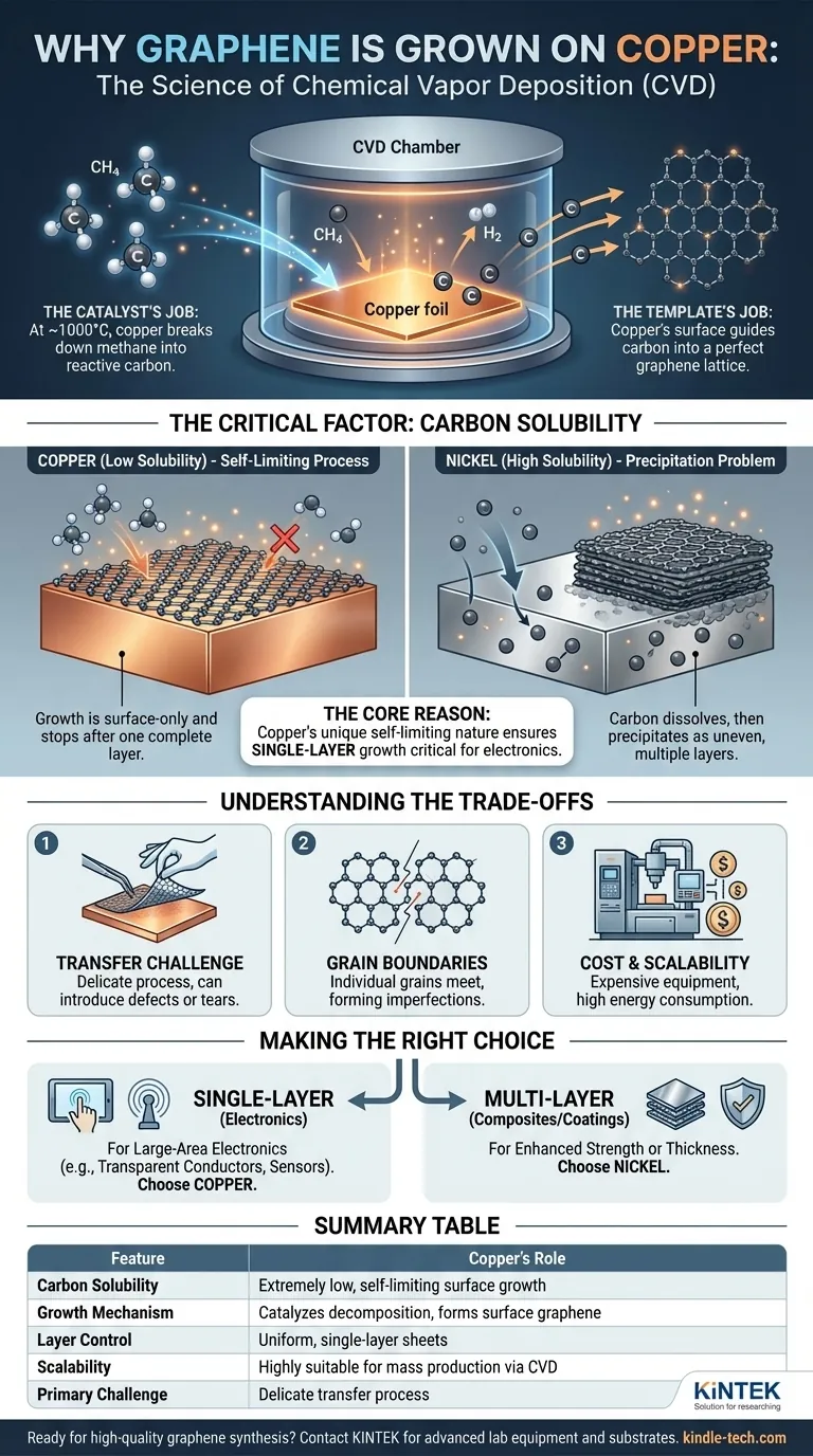
To understand why copper is so effective, we must first look at the primary method used for large-scale production: Chemical Vapor Deposition (CVD). The goal of CVD is to assemble carbon atoms into a perfect, one-atom-thick hexagonal lattice over a large area.
The Catalyst's Job: Breaking Down Carbon Sources
The process begins by heating a copper foil in a vacuum chamber and introducing a carbon-containing gas, typically methane (CH4).
At high temperatures (around 1000°C), the copper surface acts as a catalyst. It efficiently breaks down the methane molecules into reactive carbon atoms and hydrogen.
The Template's Job: Arranging Carbon Atoms
Once freed, these carbon atoms diffuse across the hot copper surface. The surface energy of the copper guides them to arrange themselves into the most stable structure possible: the hexagonal lattice of graphene. The copper acts as a perfect atomic template for this assembly.
The Critical Factor: Why Copper Outperforms Other Metals
While other metals like nickel can also catalyze this reaction, copper has a decisive advantage that makes it superior for producing the highest quality graphene needed for electronics.
The Concept of Carbon Solubility
Carbon solubility refers to the ability of a metal to absorb carbon atoms into its bulk structure at high temperatures. This single property is the most important differentiator between potential substrates.
Copper's Low Solubility: A Self-Limiting Process
Copper has exceptionally low carbon solubility. This means the carbon atoms from the broken-down methane gas remain almost exclusively on the copper's surface.
Because the growth only happens on the surface, the process is self-limiting. Once a complete, single layer of graphene covers the copper, it blocks the copper's catalytic effect. No more methane can be broken down at the surface, and growth halts. This reliably produces vast sheets of monolayer graphene.
The Nickel Alternative: A Precipitation Problem
In contrast, a metal like nickel has high carbon solubility. During CVD, carbon atoms dissolve into the bulk nickel foil, like sugar dissolving in water.
When the system cools, the nickel's ability to hold carbon decreases, and the dissolved carbon precipitates back out onto the surface. This precipitation process is difficult to control, often resulting in multiple, uneven, and inconsistent layers of graphene.
Understanding the Trade-offs
While copper is the dominant choice, it's essential to recognize the practical challenges associated with the method.
The Challenge of Transfer
The graphene grown on copper is intended for use in other applications, meaning it must be removed from the foil. This transfer process typically involves etching away the entire copper substrate, which is a delicate, multi-step process that can introduce defects, wrinkles, or tears into the graphene sheet.
Grain Boundaries and Defects
Graphene growth starts at multiple points on the copper foil simultaneously, creating individual "islands" or "grains." As these grains grow and meet, they form grain boundaries. These boundaries are imperfections in the crystal lattice that can negatively impact the material's electrical and mechanical properties.
Cost and Scalability
Although the CVD-on-copper method is lauded for its cost-effectiveness, it still requires expensive equipment, high temperatures, and vacuum conditions. While it is the best method for mass production today, scaling it for applications like consumer electronics remains a significant engineering challenge.
Making the Right Choice for Your Goal
The choice of substrate is entirely dependent on the desired quality and characteristics of the final graphene product.
- If your primary focus is large-area electronics (e.g., transparent conductors, sensors): Copper is the only viable choice because its self-limiting nature is essential for producing the required uniform, single-layer graphene.
- If your primary focus is composites or coatings where multiple layers are acceptable: Other substrates like nickel might be suitable, as the precipitation method can produce thicker graphene films that may enhance mechanical strength.
Ultimately, copper's unique ability to enforce single-layer growth is what makes it the foundational material for the future of graphene-based technologies.
Summary Table:
| Feature | Copper's Role in Graphene Growth |
|---|---|
| Carbon Solubility | Extremely low, enabling self-limiting surface growth |
| Growth Mechanism | Catalyzes methane decomposition; carbon atoms form graphene on surface only |
| Layer Control | Produces uniform, single-layer sheets critical for electronics |
| Scalability | Highly suitable for mass production via Chemical Vapor Deposition (CVD) |
| Primary Challenge | Requires delicate transfer process from copper substrate to target application |
Ready to integrate high-quality graphene into your research or production? KINTEK specializes in providing advanced lab equipment and consumables, including CVD systems and substrates tailored for graphene synthesis. Our expertise ensures you achieve precise, reproducible results for your electronic or material science applications. Contact our experts today to discuss how we can support your laboratory's innovation with reliable, cutting-edge solutions.
Visual Guide
Related Products
- CVD Diamond for Thermal Management Applications
- Graphite Vacuum Furnace Bottom Discharge Graphitization Furnace for Carbon Materials
- Carbon Graphite Plate Manufactured by Isostatic Pressing Method
- Glassy Carbon Sheet RVC for Electrochemical Experiments
- Laboratory CVD Boron Doped Diamond Materials
People Also Ask
- What are the optical properties of CVD diamond? Unlock Unmatched Performance for Demanding Applications
- How long does it take to make a CVD diamond? A Detailed Look at the Growth Timeline
- Are CVD diamonds real or fake? Discover the Truth About Lab-Grown Diamonds
- How long does it take to grow a CVD diamond? A 2-4 Week Journey to a Flawless Gem
- How long do CVD diamonds last? Discover the Truth About Their Lifespan