From a technical standpoint, Plasma-Enhanced Chemical Vapor Deposition (PECVD) is often considered superior to conventional Chemical Vapor Deposition (CVD) because it uses an energy-rich plasma, not just high heat, to drive the deposition process. This fundamental difference allows PECVD to operate at significantly lower temperatures, offering greater material compatibility, higher efficiency, and tighter control over the final film's properties.
The core distinction is not that one method is universally "better," but that PECVD's use of plasma instead of pure heat solves the primary limitation of traditional CVD: high-temperature requirements. This makes PECVD indispensable for modern applications involving heat-sensitive substrates and complex material engineering.
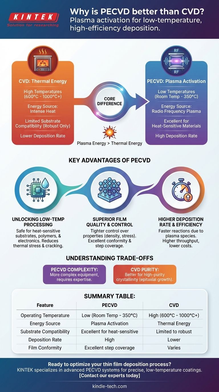
The Core Difference: Energy Source
To understand the advantages, you must first grasp the fundamental mechanism that separates these two processes. The choice between them comes down to how you supply the energy needed for the chemical reaction.
How Traditional CVD Works
Traditional thermal CVD relies exclusively on high temperatures, often ranging from 600°C to over 1000°C.
This intense heat provides the thermal energy required to break down precursor gases and allow them to react and deposit as a thin film on the substrate's surface.
The PECVD Advantage: Plasma Activation
PECVD accomplishes the same goal but at much lower temperatures (often room temperature to 350°C).
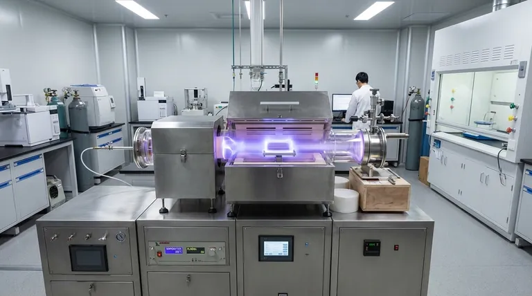
Instead of heat, it uses a radio frequency (RF) or microwave field to ignite the precursor gases into a plasma. This plasma is a highly energetic state of matter containing ions and free radicals that are extremely reactive, enabling deposition without the need for extreme thermal energy.
Key Advantages of PECVD in Practice
This shift from thermal energy to plasma activation creates several significant, practical benefits that drive its adoption in advanced manufacturing.
Unlocking Low-Temperature Processing
The most critical advantage is the ability to deposit films at low temperatures. This avoids damaging heat-sensitive substrates like plastics, organic materials, or fully fabricated electronic devices that already contain delicate circuitry.
It also reduces thermal stress between the substrate and the deposited film, especially when their thermal expansion coefficients differ. This dramatically reduces the risk of the film cracking or delaminating.
Superior Film Quality and Control
The plasma environment provides additional variables for process control, such as power, pressure, and gas flow, which are not available in thermal CVD.
This allows for tighter control over the film's properties. Engineers can precisely tune characteristics like density, stress, chemical resistance, and even optical or electrical properties by adjusting the plasma parameters.
Furthermore, PECVD is known for its excellent conformity and step coverage, meaning it can deposit a highly uniform film over complex, uneven, or three-dimensional surfaces.
Higher Deposition Rate and Efficiency
The highly reactive species in the plasma accelerate the chemical reactions. This results in significantly higher deposition rates compared to many thermal CVD processes.
Faster deposition times translate directly to higher throughput and lower operational costs in a manufacturing environment.
Understanding the Trade-offs
While powerful, PECVD is not a universal replacement for all CVD processes. An objective assessment requires acknowledging its complexities.
Equipment and Process Complexity
A PECVD system, with its RF power generators, matching networks, and advanced vacuum controls, is inherently more complex and often more expensive than a simple thermal CVD furnace.
Tuning the process also requires more expertise. Incorrect plasma parameters can lead to non-uniformity or even damage the substrate through ion bombardment, a risk not present in thermal CVD.
Film Purity and Crystallinity
For applications demanding the absolute highest film purity or a specific crystalline structure (like epitaxial growth), high-temperature thermal CVD can sometimes be superior. The high heat provides the energy for atoms to arrange themselves into a highly ordered, low-defect crystal lattice.
The lower temperatures and complex chemical environment of PECVD can sometimes result in films with higher hydrogen incorporation or an amorphous (non-crystalline) structure, which may be undesirable for certain electronic or optical applications.
Making the Right Choice for Your Application
Ultimately, the decision rests on the specific requirements of your substrate, your desired film properties, and your manufacturing goals.
- If your primary focus is depositing on heat-sensitive substrates (like polymers or pre-fabricated electronics): PECVD is the clear and often only viable choice due to its low-temperature processing.
- If your primary focus is achieving high deposition speed and throughput: PECVD often provides a significant advantage due to its plasma-accelerated reaction rates.
- If your primary focus is creating a highly uniform coating over complex, 3D topography: PECVD's excellent step coverage makes it the superior choice for ensuring complete and even coating.
- If your primary focus is growing a high-purity, single-crystal film on a robust substrate: Traditional thermal CVD may be a more reliable and straightforward method.
By understanding the core difference between thermal and plasma activation, you are empowered to select the precise deposition tool for your specific engineering goal.
Summary Table:
| Feature | PECVD | CVD |
|---|---|---|
| Operating Temperature | Low (Room Temp - 350°C) | High (600°C - 1000°C+) |
| Energy Source | Plasma Activation | Thermal Energy |
| Substrate Compatibility | Excellent for heat-sensitive materials | Limited to high-temperature substrates |
| Deposition Rate | High | Lower |
| Film Conformity | Excellent step coverage | Varies |
Ready to optimize your thin film deposition process? KINTEK specializes in advanced lab equipment, including PECVD systems, to help you achieve precise, low-temperature coatings for heat-sensitive substrates. Our expertise ensures you get the right solution for higher throughput and superior film quality. Contact our experts today to discuss how we can enhance your laboratory's capabilities!
Visual Guide
Related Products
- Inclined Rotary Plasma Enhanced Chemical Vapor Deposition PECVD Equipment Tube Furnace Machine
- Chemical Vapor Deposition CVD Equipment System Chamber Slide PECVD Tube Furnace with Liquid Gasifier PECVD Machine
- Inclined Rotary Plasma Enhanced Chemical Vapor Deposition PECVD Equipment Tube Furnace Machine
- RF PECVD System Radio Frequency Plasma-Enhanced Chemical Vapor Deposition RF PECVD
- Multi Heating Zones CVD Tube Furnace Machine Chemical Vapor Deposition Chamber System Equipment
People Also Ask
- What are the advantages of plasma enhanced chemical vapor deposition? Enable Low-Temperature, High-Quality Film Deposition
- What is plasma enhanced chemical vapor deposition PECVD equipment? A Guide to Low-Temperature Thin Film Deposition
- Why is a PECVD system required for vertical graphene synthesis? Master Directional Control for 3D Nanostructures
- What are the benefits of plasma enhanced CVD? Achieve High-Quality, Low-Temperature Film Deposition
- What is plasma enhanced chemical vapour deposition PECVD used for? Enable Low-Temp Thin Films for Electronics & Solar


