Knowledge Why is thin film used? To Engineer Superior Surface Properties on Any Material
Author avatar

Tech Team · Kintek Solution

Updated 4 days ago

Why is thin film used? To Engineer Superior Surface Properties on Any Material


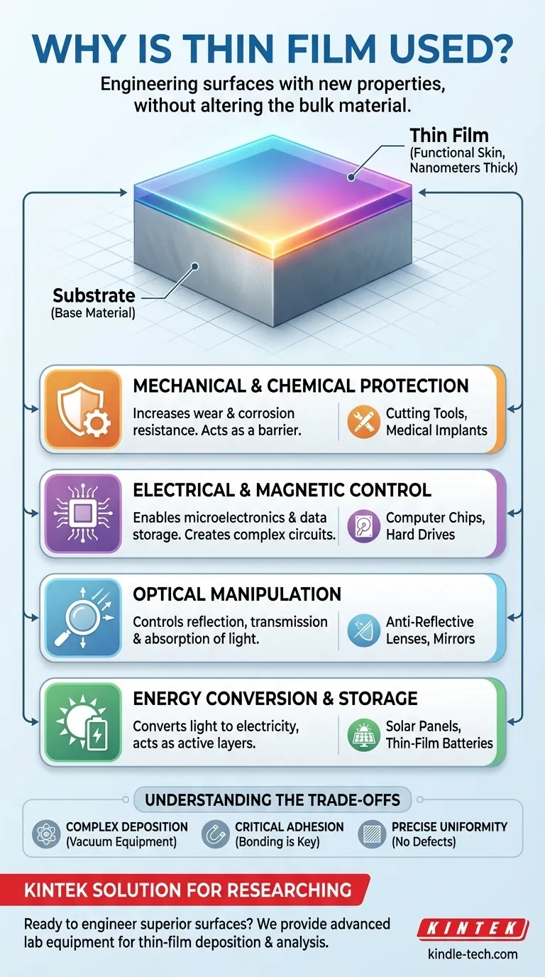
In short, thin films are used to add new properties to the surface of a material. These engineered layers are applied to a base material, known as a substrate, to enhance its performance or grant it entirely new capabilities—such as making it more durable, electrically conductive, or able to interact with light in specific ways.

The core reason for using thin films is to strategically engineer the surface of an object without altering its bulk properties. This allows for the creation of high-performance products by combining the cost-effectiveness or structural integrity of a base material with the specialized functions of a microscopic surface layer.

Why is thin film used? To Engineer Superior Surface Properties on Any Material

The Core Principle: Engineering a Surface

Think of a thin film not as a standalone object, but as a functional "skin" applied to a larger structure. This approach is fundamental to modern materials science and engineering.

Substrate and Film: A Symbiotic Relationship

A substrate is the base material, chosen for its structural properties, cost, or other core attributes. The thin film is the meticulously deposited layer, often only nanometers or micrometers thick, that provides a specialized surface function.

This combination allows engineers to create materials that are, for example, as strong as steel but also highly reflective, or as flexible as plastic but also capable of generating electricity from light.

Why Not Make the Whole Object from the Film Material?

In many cases, the material used for the thin film is expensive, rare, or lacks the necessary structural strength for the application. Applying it as a thin layer is far more efficient and economical than constructing the entire device from that material.

Key Functional Benefits of Thin Films

The versatility of thin films comes from the wide range of properties they can introduce. These functions can be grouped into several key categories.

Enhancing Mechanical and Chemical Properties

One of the most common uses for thin films is protection. They act as a barrier between the substrate and the environment.

This includes providing superior resistance to wear and corrosion, which is critical for extending the life of cutting tools, engine components, and medical implants. They also increase durability and can improve the adhesion of subsequent layers.

Modifying Electrical and Magnetic Behavior

Thin films are the building blocks of the digital world. Layers of conductive, insulating, and semi-conductive materials are deposited to create complex circuits.

These films are essential for microelectronic devices like the transistors in computer processors, magnetic storage media like hard drives, and components for advanced thin-film batteries.

Manipulating Light and Optics

Thin films give us precise control over how light reflects, transmits, or is absorbed by a surface.

This is the principle behind anti-reflective coatings on eyeglass lenses and camera lenses, the reflective layers on household mirrors, and specialized optical filters used in scientific instruments. They are also used for simple cosmetic improvements to enhance a product's appearance.

Enabling Energy Conversion and Storage

Thin films are critical for renewable energy technologies. They are the active layers in many photovoltaic cells (solar panels), responsible for converting light energy into electrical power.

They also play a key role in the development of next-generation thin-film batteries and other energy storage devices.

Understanding the Trade-offs

While powerful, the application of thin films is a highly technical process with specific challenges.

The Complexity of Deposition

Applying a thin film is not like painting. It requires sophisticated vacuum process equipment that uses methods like Physical Vapor Deposition (PVD) or Chemical Vapor Deposition (CVD). This machinery is complex and represents a significant investment.

The Critical Need for Adhesion

A thin film is only effective if it bonds perfectly to the substrate. If adhesion fails, the film can peel or flake off, completely negating its benefits. Ensuring a clean surface and the right process parameters is crucial.

The Challenge of Uniformity

For applications in optics or microelectronics, the film must be perfectly uniform in thickness and free of microscopic defects or pinholes. Achieving this level of precision across a large surface area is a significant engineering challenge.

Making the Right Choice for Your Goal

The reason for using a thin film depends entirely on the problem you are trying to solve.

  • If your primary focus is protection and durability: Thin films are used as hard, corrosion-resistant coatings to dramatically extend the lifespan of tools and components.
  • If your primary focus is advanced electronic or optical functionality: Thin films are the fundamental building blocks used to create everything from computer chips to anti-reflection lenses.
  • If your primary focus is energy conversion or storage: Thin films are the active layers essential for creating modern solar cells and next-generation batteries.

Ultimately, thin-film technology allows us to create materials with capabilities that far exceed what any single substance could provide on its own.

Summary Table:

Key Function Primary Benefit Common Applications
Mechanical/Chemical Protection Increases wear & corrosion resistance Cutting tools, medical implants
Electrical/Magnetic Control Enables microelectronics & data storage Computer chips, hard drives
Optical Manipulation Controls reflection, transmission, absorption Anti-reflective lenses, mirrors
Energy Conversion & Storage Converts light to electricity, stores energy Solar panels, thin-film batteries

Ready to engineer superior surface properties for your products? KINTEK specializes in advanced lab equipment and consumables for thin-film deposition and analysis. Our solutions help you develop durable coatings, sophisticated electronics, and efficient energy devices. Contact our experts today to discuss how we can support your laboratory's thin-film innovation.

Visual Guide

Why is thin film used? To Engineer Superior Surface Properties on Any Material Visual Guide

Related Products

People Also Ask

Related Products

RF PECVD System Radio Frequency Plasma-Enhanced Chemical Vapor Deposition RF PECVD

RF PECVD System Radio Frequency Plasma-Enhanced Chemical Vapor Deposition RF PECVD

RF-PECVD is an acronym for "Radio Frequency Plasma-Enhanced Chemical Vapor Deposition." It deposits DLC (Diamond-like carbon film) on germanium and silicon substrates. It is utilized in the 3-12um infrared wavelength range.

Chemical Vapor Deposition CVD Equipment System Chamber Slide PECVD Tube Furnace with Liquid Gasifier PECVD Machine

Chemical Vapor Deposition CVD Equipment System Chamber Slide PECVD Tube Furnace with Liquid Gasifier PECVD Machine

KT-PE12 Slide PECVD System: Wide power range, programmable temp control, fast heating/cooling with sliding system, MFC mass flow control & vacuum pump.

915MHz MPCVD Diamond Machine Microwave Plasma Chemical Vapor Deposition System Reactor

915MHz MPCVD Diamond Machine Microwave Plasma Chemical Vapor Deposition System Reactor

915MHz MPCVD Diamond Machine and its multi-crystal effective growth, the maximum area can reach 8 inches, the maximum effective growth area of single crystal can reach 5 inches. This equipment is mainly used for the production of large-size polycrystalline diamond films, the growth of long single crystal diamonds, the low-temperature growth of high-quality graphene, and other materials that require energy provided by microwave plasma for growth.

CVD Diamond Cutting Tool Blanks for Precision Machining

CVD Diamond Cutting Tool Blanks for Precision Machining

CVD Diamond Cutting Tools: Superior Wear Resistance, Low Friction, High Thermal Conductivity for Non-Ferrous Materials, Ceramics, Composites Machining

Multi Heating Zones CVD Tube Furnace Machine Chemical Vapor Deposition Chamber System Equipment

Multi Heating Zones CVD Tube Furnace Machine Chemical Vapor Deposition Chamber System Equipment

KT-CTF14 Multi Heating Zones CVD Furnace - Precise Temperature Control and Gas Flow for Advanced Applications. Max temp up to 1200℃, 4 channels MFC mass flow meter, and 7" TFT touch screen controller.

CVD Diamond Domes for Industrial and Scientific Applications

CVD Diamond Domes for Industrial and Scientific Applications

Discover CVD diamond domes, the ultimate solution for high-performance loudspeakers. Made with DC Arc Plasma Jet technology, these domes deliver exceptional sound quality, durability, and power handling.

Customer Made Versatile CVD Tube Furnace Chemical Vapor Deposition Chamber System Equipment

Customer Made Versatile CVD Tube Furnace Chemical Vapor Deposition Chamber System Equipment

Get your exclusive CVD furnace with KT-CTF16 Customer Made Versatile Furnace. Customizable sliding, rotating, and tilting functions for precise reactions. Order now!

Split Chamber CVD Tube Furnace with Vacuum Station Chemical Vapor Deposition System Equipment Machine

Split Chamber CVD Tube Furnace with Vacuum Station Chemical Vapor Deposition System Equipment Machine

Efficient split chamber CVD furnace with vacuum station for intuitive sample checking and quick cooling. Up to 1200℃ max temperature with accurate MFC mass flowmeter control.

1200℃ Split Tube Furnace with Quartz Tube Laboratory Tubular Furnace

1200℃ Split Tube Furnace with Quartz Tube Laboratory Tubular Furnace

KT-TF12 split tube furnace: high-purity insulation, embedded heating wire coils, and max. 1200C. Widely used for new materials and chemical vapour deposition.

Vertical High Temperature Graphite Vacuum Graphitization Furnace

Vertical High Temperature Graphite Vacuum Graphitization Furnace

Vertical high temperature graphitization furnace for carbonization and graphitization of carbon materials up to 3100℃.Suitable for shaped graphitization of carbon fiber filaments and other materials sintered in a carbon environment.Applications in metallurgy, electronics, and aerospace for producing high-quality graphite products like electrodes and crucibles.

Large Vertical Graphite Vacuum Graphitization Furnace

Large Vertical Graphite Vacuum Graphitization Furnace

A large vertical high-temperature graphitization furnace is a type of industrial furnace used for the graphitization of carbon materials, such as carbon fiber and carbon black. It is a high-temperature furnace that can reach temperatures of up to 3100°C.

1700℃ Controlled Atmosphere Furnace Nitrogen Inert Atmosphere Furnace

1700℃ Controlled Atmosphere Furnace Nitrogen Inert Atmosphere Furnace

KT-17A Controlled atmosphere furnace: 1700℃ heating, vacuum sealing technology, PID temperature control, and versatile TFT smart touch screen controller for laboratory and industrial use.

1400℃ Controlled Atmosphere Furnace with Nitrogen and Inert Atmosphere

1400℃ Controlled Atmosphere Furnace with Nitrogen and Inert Atmosphere

Achieve precise heat treatment with KT-14A controlled atmosphere furnace. Vacuum sealed with a smart controller, it's ideal for lab and industrial use up to 1400℃.

Vacuum Heat Treat and Molybdenum Wire Sintering Furnace for Vacuum Sintering

Vacuum Heat Treat and Molybdenum Wire Sintering Furnace for Vacuum Sintering

A vacuum molybdenum wire sintering furnace is a vertical or bedroom structure, which is suitable for withdrawal, brazing, sintering and degassing of metal materials under high vacuum and high temperature conditions. It is also suitable for dehydroxylation treatment of quartz materials.

Vacuum Dental Porcelain Sintering Furnace

Vacuum Dental Porcelain Sintering Furnace

Get precise and reliable results with KinTek's Vacuum Porcelain Furnace. Suitable for all porcelain powders, it features hyperbolic ceramic furnace function, voice prompt, and automatic temperature calibration.

Ultra-High Temperature Graphite Vacuum Graphitization Furnace

Ultra-High Temperature Graphite Vacuum Graphitization Furnace

The ultra-high temperature graphitization furnace utilizes medium frequency induction heating in a vacuum or inert gas environment. The induction coil generates an alternating magnetic field, inducing eddy currents in the graphite crucible, which heats up and radiates heat to the workpiece, bringing it to the desired temperature. This furnace is primarily used for graphitization and sintering of carbon materials, carbon fiber materials, and other composite materials.

High-Purity Titanium Foil and Sheet for Industrial Applications

High-Purity Titanium Foil and Sheet for Industrial Applications

Titanium is chemically stable, with a density of 4.51g/cm3, which is higher than aluminum and lower than steel, copper, and nickel, but its specific strength ranks first among metals.

Custom PTFE Wafer Holders for Lab and Semiconductor Processing

Custom PTFE Wafer Holders for Lab and Semiconductor Processing

This is a high-purity, custom-machined PTFE (Teflon) holder, expertly designed for the secure handling and processing of delicate substrates like conductive glass, wafers, and optical components.

Circulating Water Vacuum Pump for Laboratory and Industrial Use

Circulating Water Vacuum Pump for Laboratory and Industrial Use

Efficient circulating water vacuum pump for labs - oil-free, corrosion-resistant, quiet operation. Multiple models available. Get yours now!

Non Consumable Vacuum Arc Induction Melting Furnace

Non Consumable Vacuum Arc Induction Melting Furnace

Explore the benefits of Non-Consumable Vacuum Arc Furnace with high melting point electrodes. Small, easy to operate & eco-friendly. Ideal for laboratory research on refractory metals & carbides.


Leave Your Message