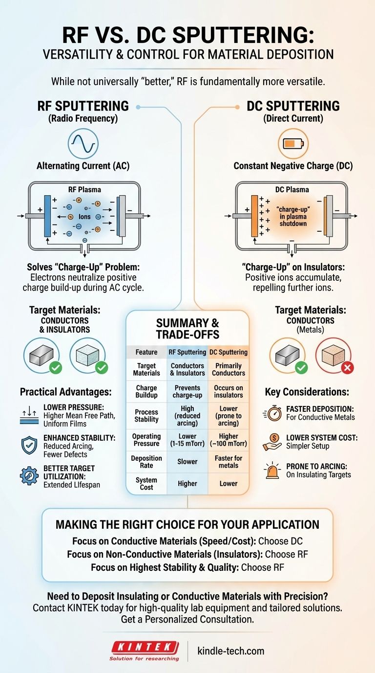
In essence, RF sputtering is not universally "better" than DC sputtering, but it is fundamentally more versatile. The primary advantage of Radio Frequency (RF) sputtering is its ability to deposit insulating (dielectric) materials, a task impossible for standard Direct Current (DC) systems. This capability stems from its use of an alternating current, which prevents the process-killing charge build-up that occurs on non-conductive targets in a DC environment.
The choice between RF and DC sputtering is not a matter of one being superior, but of selecting the right tool for the job. DC sputtering is the workhorse for conductive metals due to its speed and simplicity, while RF sputtering provides the critical capability to work with insulators and offers a more stable, refined process environment.
The Core Difference: How Power Source Dictates Capability
The fundamental distinction between the two techniques lies in the type of power applied to create the plasma. This single choice has profound implications for the types of materials you can work with.
DC Sputtering: The Problem of "Charge-Up"
In DC sputtering, the target material is given a large, constant negative charge. This attracts positive gas ions (like Argon+) from the plasma, which strike the target with enough force to dislodge atoms for deposition.
This process works perfectly for conductive targets (metals) because the target can dissipate the positive charge from the arriving ions.
However, if the target is an insulator (like a ceramic), the positive charge from the ions accumulates on its surface. This "charge-up" effect quickly repels any more positive ions, effectively shutting down the sputtering process and often leading to damaging plasma arcs.
RF Sputtering: The Alternating Current Solution
RF sputtering solves the charge-up problem by using a high-frequency alternating current (AC), typically at 13.56 MHz.
During the negative half of the AC cycle, the target behaves like a DC target, attracting positive ions for sputtering. Crucially, during the brief positive half-cycle, the target attracts a flood of highly mobile electrons from the plasma.
These electrons instantly neutralize the positive charge that built up during the sputtering phase. This rapid switching prevents charge accumulation, allowing for the continuous and stable sputtering of insulating materials.
The Practical Advantages of the RF Process
Beyond enabling insulator deposition, the nature of an RF plasma provides several secondary benefits that lead to a more controlled and stable process.
Sustaining Plasma at Lower Pressure
RF energy is significantly more efficient at ionizing gas and sustaining a plasma than a DC field. This allows RF systems to operate at much lower working pressures (1-15 mTorr) compared to DC systems (often near 100 mTorr).
The Benefit: Higher Mean Free Path
Operating at a lower pressure means there are far fewer gas atoms in the chamber. This increases the mean free path—the average distance a sputtered atom can travel before colliding with a gas particle.
A longer mean free path results in the sputtered material traveling in a more direct line from the target to your substrate. This can improve film density and deposition efficiency.
Enhanced Process Stability
The alternating field of RF sputtering prevents the "disappearing anode" effect common in DC systems, where chamber walls can become coated with an insulating layer and disrupt the plasma.
By also eliminating the charge-up that causes arcing on insulating targets, RF sputtering provides a dramatically more stable process, leading to more uniform films with fewer defects.
Improved Target Utilization
Many DC systems, particularly magnetron sputtering, use magnets to confine the plasma, leading to heavy erosion in a specific "race track" pattern on the target. This wastes material and reduces the target's lifespan.
The plasma in an RF system is often more diffuse, engaging a larger surface area of the target. This results in more even erosion, extending the life of the target and maximizing the use of your source material.
Understanding the Trade-offs
While RF sputtering is more versatile, it is not always the best choice. Acknowledging its limitations is key to making a sound technical decision.
Deposition Rate: The Speed Advantage of DC
For depositing conductive metals, DC magnetron sputtering is typically faster than RF sputtering. The RF process includes a non-sputtering half-cycle for charge neutralization, which slightly reduces the overall deposition rate compared to the continuous bombardment in a DC system.
System Complexity and Cost
RF sputtering systems are inherently more complex and expensive. They require a dedicated RF power supply and an impedance-matching network—a critical component that fine-tunes the electrical circuit to ensure maximum power is transferred to the plasma, not reflected back to the source. This adds significant cost and complexity compared to a simpler DC setup.
Making the Right Choice for Your Application
Your choice should be dictated entirely by your material requirements and project goals.
- If your primary focus is depositing conductive materials (metals) at high speed and low cost: Standard DC magnetron sputtering is almost always the more efficient and economical choice.
- If your primary focus is depositing non-conductive materials (ceramics, dielectrics, polymers): RF sputtering is the necessary and correct technology for the task.
- If your primary focus is achieving the highest process stability and film quality, even for metals: Consider RF sputtering for its advantages in lower-pressure operation and reduced potential for arcing.
Ultimately, understanding the fundamental physics of each process empowers you to select the technology that best aligns with your material and desired outcome.
Summary Table:
| Feature | RF Sputtering | DC Sputtering |
|---|---|---|
| Target Materials | Conductors & Insulators | Primarily Conductors |
| Charge Buildup | Prevents charge-up | Occurs on insulators |
| Process Stability | High (reduced arcing) | Lower (prone to arcing) |
| Operating Pressure | Lower (1-15 mTorr) | Higher (~100 mTorr) |
| Deposition Rate | Slower | Faster for metals |
| System Cost | Higher | Lower |
Need to Deposit Insulating or Conductive Materials with Precision?
Choosing the right sputtering technology is critical for your research or production outcomes. KINTEK specializes in providing high-quality lab equipment and consumables, including both RF and DC sputtering systems tailored to your specific material science needs.
Our experts can help you:
- Select the ideal system for your target materials (metals, ceramics, dielectrics)
- Achieve superior film quality with stable, controlled processes
- Maximize your investment with the right tool for your application
Contact us today to discuss your project requirements and discover how KINTEK's solutions can enhance your laboratory's capabilities.
Get a Personalized Consultation
Visual Guide
Related Products
- RF PECVD System Radio Frequency Plasma-Enhanced Chemical Vapor Deposition RF PECVD
- Horizontal High Temperature Graphite Vacuum Graphitization Furnace
- Spark Plasma Sintering Furnace SPS Furnace
- Automatic Laboratory Hydraulic Press for XRF & KBR Pellet Press
- Electron Beam Evaporation Coating Oxygen-Free Copper Crucible and Evaporation Boat
People Also Ask
- What is plasma CVD? Unlock Low-Temperature Thin Film Deposition for Sensitive Materials
- What is an example of PECVD? RF-PECVD for High-Quality Thin Film Deposition
- What is plasma enhanced chemical Vapour deposition process used for fabrication of? A Guide to Low-Temperature Thin Films
- How does plasma enhance CVD? Unlock Low-Temperature, High-Quality Film Deposition
- How does Radio Frequency Enhanced Plasma Chemical Vapour Deposition (RF-PECVD) work? Learn the Core Principles


