Lab Materials
high purity gold (Au) sputtering target / powder / wire / block / granule
Item Number : LM-AU
Price varies based on specs and customizations
- Chemical Formula
- Au
- Purity
- 4N-5N
- Shape
- discs / wire / block / powder / plates / column targets / step target / custom-made

Shipping:
Contact us to get shipping details Enjoy On-time Dispatch Guarantee.
We offer gold (AU) materials for laboratory use at reasonable prices. Our expertise lies in producing and tailoring gold (AU) materials of different purities, shapes, and sizes to suit your unique requirements.
We provide a range of specifications and sizes for sputtering targets (circular, square, tubular, irregular), coating materials, cylinders, cones, particles, foils, powders, 3D printing powders, nanometer powders, wire rods, ingots, and blocks etc.
Main Products
- Gold particles 99.999%, Application: Thermal Evaporation, Electron Beam Evaporation
- Gold target 99.99%, Application: Magnetron Sputtering Coating
- SEM gold target 99.99%, Application: Scanning electron microscope SEM equipment
- Gold wire 99.999%, Application: thermal evaporation, etc.
- Bonding gold wire 99.99%, Application: LED semiconductor packaging
- Gold nuggets 99.99%, Application: Alloy smelting industry, etc.
- Gold sequin 99.99%, Application: evaporation, melting, etc.
- Gold rod 99.999%, Application: evaporation, melting, etc.
Details


About Gold (Au)
Gold is widely used in coinage and is a standard in most modern monetary systems. Additionally, it is extensively used in jewelry, dental restorations, and plating. Its inert and good infrared reflecting properties make it an excellent choice for coating certain space satellites.
The use of gold in electronics has seen significant growth, particularly in telecommunications, information technology, and safety-critical applications. Computers usually have gold-plated edge connectors, and gold bonding wires are widely used in semiconductor packages. Gold thick film inks are also applied in the fabrication of hybrid circuits. Gold's excellent solder wetting properties make it ideal for forming a protective layer on copper laminate printed circuit boards.
Gold is available in various forms, including metal, compounds with purities ranging from 99% to 99.999%, and sputtering targets for evaporation source material purposes. Gold nanoparticles and nanopowders are also available, and gold oxides are available in powder and dense pellet form for optical coating and thin film applications. Gold is also available in soluble forms, including chlorides, nitrates, and acetates, which can be manufactured as solutions at specified stoichiometries.
Ingredient Quality Control
- Raw material composition analysis
- Through the use of equipment such as ICP and GDMS, the content of metal impurities is detected and analyzed to ensure that it meets the purity standard;
Non-metallic impurities are detected by equipment such as carbon and sulfur analyzers, nitrogen and oxygen analyzers. - Metallographic flaw detection analysis
- The target material is inspected using flaw detection equipment to ensure that there are no defects or shrinkage holes inside the product;
Through metallographic testing, the internal grain structure of the target material is analyzed to ensure that the grains are fine and dense. - Appearance and dimension inspection
- Product dimensions are measured using micrometers and precision calipers to ensure compliance with drawings;
The surface finish and cleanliness of the product are measured using a surface cleanliness meter.
Conventional Sputtering Target Sizes
- Preparation process
- hot isostatic pressing, vacuum melting, etc.
- Sputtering target shape
- plane sputtering target, multi-arc sputtering target, step sputtering target, special-shaped sputtering target
- Round sputtering target size
- Diameter: 25.4mm / 50mm / 50.8mm / 60mm / 76.2mm / 80mm / 100mm / 101.6mm / 152.4mm
Thickness: 3mm / 4mm / 5mm / 6mm / 6.35mm
Size can be customized. - Square sputtering target size
- 50×50×3mm / 100×100×4mm / 300×300×5mm, size can be customized
Available Metal Forms
Metal Forms Details
We manufacture almost all the metals listed on the periodic table in a wide range of forms and purities, as well as standard sizes and dimensions. We can also produce custom-made products to meet specific customer requirements, such as size, shape, surface area, composition, and more. The following list provides a sample of the forms we offer, but it is not exhaustive. If you need laboratory consumables, please contact us directly to request a quote.
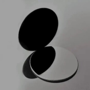
- Flat/Planar Forms: Board, Film, Foil, Microfoil, Microleaf, Paper, Plate, Ribbon, Sheet, Strip, Tape, Wafer
- Preformed Shapes: Anodes, Balls, Bands, Bars, Boats, Bolts, Briquettes, Cathodes, Circles, Coils, Crucibles, Crystals, Cubes, Cups, Cylinders, Discs, Electrodes, Fibers, Filaments, Flanges, Grids, Lenses, Mandrels, Nuts, Parts, Prisms, Pucks, Rings, Rods, Shapes, Shields, Sleeves, Springs, Squares, Sputtering Targets, Sticks, Tubes, Washers, Windows, Wires
- Microsizes: Beads, Bits, Capsules, Chips, Coins, Dust, Flakes, Grains, Granules, Micropowder, Needles, Particles, Pebbles, Pellets, Pins, Pills, Powder, Shavings, Shot, Slugs, Spheres, Tablets
- Macrosizes: Billets, Chunks, Cuttings, Fragments, Ingots, Lumps, Nuggets, Pieces, Punchings, Rocks, Scraps, Segments, Turnings
- Porous and Semi-Porous: Fabric, Foam, Gauze, Honeycomb, Mesh, Sponge, Wool
- Nanoscale: Nanoparticles, Nanopowders, Nanofoils, Nanotubes, Nanorods, Nanoprisms
- Others: Concentrate, Ink, Paste, Precipitate, Residue, Samples, Specimens
KinTek specializes in the manufacturing of high-purity and ultra-high-purity materials with a purity range of 99.999% (5N), 99.9999% (6N), 99.99995% (6N5), and in some cases, up to 99.99999% (7N). Our materials are available in specific grades, including UP/UHP, semiconductor, electronic, deposition, fiber optic, and MBE grades. Our high-purity metals, oxides, and compounds are specifically crafted to meet the rigorous demands of high-technology applications and are ideal for use as dopants and precursor materials for thin film deposition, crystal growth of semiconductors, and synthesis of nanomaterials. These materials find use in advanced microelectronics, solar cells, fuel cells, optical materials, and other cutting-edge applications.
Packaging
We use vacuum packaging for our high-purity materials, and each material has specific packaging tailored to its unique characteristics. For instance, our Hf sputter target is externally tagged and labeled to facilitate efficient identification and quality control. We take great care to prevent any damage that could occur during storage or transportation.
FAQ
What Are High Purity Metals?
What Are High Purity Metals Used For?
What Are The Benefits Of Using High-purity Metals?
Which Industries Commonly Use High-purity Metals?
4.9
out of
5
Their gold sputtering targets are of exceptional quality, leading to remarkable thin film uniformity and adhesion.
4.7
out of
5
The gold sputtering targets from KINTEK SOLUTION are highly pure, resulting in minimal defects and enhanced film properties.
4.8
out of
5
KINTEK SOLUTION's gold sputtering targets have a smooth surface finish, minimizing defects and improving film quality.
4.6
out of
5
These gold sputtering targets are durable and long-lasting, reducing the frequency of target replacements and downtime.
4.9
out of
5
The gold sputtering targets from KINTEK SOLUTION provide excellent value for money, delivering superior performance at a competitive price.
4.7
out of
5
KINTEK SOLUTION's gold sputtering targets are easy to integrate into our existing systems, ensuring a seamless production process.
4.8
out of
5
The technical support team at KINTEK SOLUTION is knowledgeable and responsive, providing valuable assistance whenever needed.
4.6
out of
5
KINTEK SOLUTION's gold sputtering targets are consistently reliable, ensuring stable and predictable thin film deposition.
4.9
out of
5
The gold sputtering targets from KINTEK SOLUTION are shipped promptly, meeting our tight production schedules.
4.7
out of
5
KINTEK SOLUTION's gold sputtering targets are compatible with a wide range of deposition techniques, enhancing our versatility.
4.8
out of
5
The gold sputtering targets from KINTEK SOLUTION are meticulously manufactured, ensuring exceptional consistency and uniformity.
4.6
out of
5
KINTEK SOLUTION's gold sputtering targets are backed by comprehensive documentation, facilitating seamless integration and operation.
4.9
out of
5
The gold sputtering targets from KINTEK SOLUTION are customizable, allowing us to tailor them to our specific requirements.
4.7
out of
5
KINTEK SOLUTION's gold sputtering targets are manufactured using advanced technology, resulting in superior film properties.
4.8
out of
5
The gold sputtering targets from KINTEK SOLUTION are packaged with care, ensuring they arrive in pristine condition.
4.6
out of
5
KINTEK SOLUTION's gold sputtering targets are competitively priced, providing excellent value for our investment.
4.9
out of
5
The gold sputtering targets from KINTEK SOLUTION are easy to handle and install, minimizing downtime during maintenance.
4.7
out of
5
KINTEK SOLUTION's gold sputtering targets are RoHS compliant, ensuring they meet environmental regulations.
4.8
out of
5
The gold sputtering targets from KINTEK SOLUTION are backed by a comprehensive warranty, providing peace of mind.
4.6
out of
5
KINTEK SOLUTION's gold sputtering targets are a valuable addition to our laboratory, enabling us to achieve exceptional results.
REQUEST A QUOTE
Our professional team will reply to you within one business day. Please feel free to contact us!
Related Products
High Purity Platinum (Pt) Sputtering Target / Powder / Wire / Block / Granule
High purity Platinum (Pt) sputtering targets, powders, wires, blocks, and granules at affordable prices. Tailored to your specific needs with diverse sizes and shapes available for various applications.
High Purity Germanium (Ge) Sputtering Target / Powder / Wire / Block / Granule
Get high-quality gold materials for your laboratory needs at affordable prices. Our custom-made gold materials come in various shapes, sizes, and purities to fit your unique requirements. Explore our range of sputtering targets, coating materials, foils, powders, and more.
High Purity Aluminum (Al) Sputtering Target / Powder / Wire / Block / Granule
Get high-quality Aluminum (Al) materials for laboratory use at affordable prices. We offer customized solutions including sputtering targets, powders, foils, ingots & more to meet your unique needs. Order now!
High Purity Silver (Ag) Sputtering Target / Powder / Wire / Block / Granule
Looking for affordable Silver (Ag) materials for your laboratory needs? Our experts specialize in producing varying purities, shapes, and sizes to fit your unique requirements.
Discover high-quality gold sheet electrodes for safe and durable electrochemical experiments. Choose from complete models or customize to meet your specific needs.
High Purity Tungsten (W) Sputtering Target / Powder / Wire / Block / Granule
Find high-quality Tungsten (W) materials for your laboratory needs at affordable prices. We offer customized purities, shapes, and sizes of sputtering targets, coating materials, powders, and more.
High Purity Palladium (Pd) Sputtering Target / Powder / Wire / Block / Granule
Looking for affordable Palladium materials for your lab? We offer custom solutions with varying purities, shapes, and sizes - from sputtering targets to nanometer powders and 3D printing powders. Browse our range now!
High Purity Zinc (Zn) Sputtering Target / Powder / Wire / Block / Granule
Find high-quality Zinc (Zn) materials for laboratory use at affordable prices. Our experts produce and customize materials of different purities, shapes, and sizes to suit your needs. Browse our range of sputtering targets, coating materials, and more.
High Purity Rhodium (Rh) Sputtering Target / Powder / Wire / Block / Granule
Get high-quality Rhodium materials for your lab needs at great prices. Our expert team produces and customizes Rhodium of various purities, shapes, and sizes to fit your unique requirements. Choose from a wide range of products, including sputtering targets, coating materials, powders, and more.

Electron Beam Evaporation Coating / Gold Plating / Tungsten Crucible / Molybdenum Crucible
These crucibles act as containers for the gold material evaporated by the electron evaporation beam while precisely directing the electron beam for precise deposition.
Platinum Sheet Platinum Electrode
Platinum sheet is composed of platinum, which is also one of the refractory metals. It is soft and can be forged, rolled and drawn into rod, wire, plate, tube and wire.
High Purity Antimony (Sb) Sputtering Target / Powder / Wire / Block / Granule
Get high-quality Antimony (Sb) materials tailored to your specific needs. We offer a wide range of shapes and sizes at reasonable prices. Browse our sputtering targets, powders, foils, and more.
Infrared thermal imaging / infrared temperature measurement double-sided coated germanium (Ge) lens
Germanium lenses are durable, corrosion-resistant optical lenses suited for harsh environments and applications exposed to the elements.

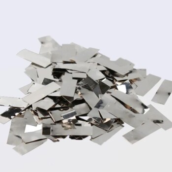
High Purity Metal Sheets - Gold / Platinum / copper / iron etc...
Elevate your experiments with our high-purity sheet metal. Gold, platinum, copper, iron, and more. Perfect for electrochemistry and other fields.
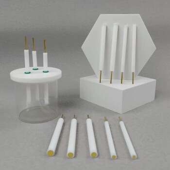
Looking for a high-quality gold disc electrode for your electrochemical experiments? Look no further than our top-of-the-line product.

High temperature resistant optical quartz glass sheet
Discover the power of optical glass sheets for precise light manipulation in telecommunications, astronomy, and beyond. Unlock advancements in optical technology with exceptional clarity and tailored refractive properties.
High Purity Lead (Pb) Sputtering Target / Powder / Wire / Block / Granule
Looking for high-quality Lead (Pb) materials for your laboratory needs? Look no further than our specialized selection of customizable options, including sputtering targets, coating materials, and more. Contact us today for competitive pricing!

Optical quartz plate JGS1 / JGS2 / JGS3
The quartz plate is a transparent, durable, and versatile component widely used in various industries. Made from high-purity quartz crystal, it exhibits excellent thermal and chemical resistance.

Diamond optical windows: exceptional broad band infrared transparency, excellent thermal conductivity & low scattering in infrared, for high-power IR laser & microwave windows applications.
There are very few harmful impurities in the chemical composition of zinc foil, and the surface of the product is straight and smooth; it has good comprehensive properties, processability, electroplating colorability, oxidation resistance and corrosion resistance, etc.

High Purity Tellurium (Te) Sputtering Target / Powder / Wire / Block / Granule
Discover our range of high-quality Tellurium (Te) materials for laboratory use at affordable prices. Our expert team produces custom sizes and purities to fit your unique needs. Shop sputtering targets, powders, ingots, and more.
High Purity Indium (In) Sputtering Target / Powder / Wire / Block / Granule
Looking for high-quality Indium materials for laboratory use? Look no further! Our expertise lies in producing tailored Indium materials of varying purities, shapes, and sizes. We offer a wide range of Indium products to suit your unique requirements. Order now at reasonable prices!
Related Articles

How To Turn XRF analysis sample preparation Into Success
In X-ray fluorescence (XRF) analysis, sample preparation is an important step because it can significantly impact both the quality and the efficiency of the analysis.
Application, Preparation, and Recovery of Precious Metal Targets in Semiconductor Manufacturing
Discusses the use, preparation, and recycling of precious metal targets in semiconductor manufacturing.
Electron Beam Evaporation Coating Technology and Material Selection
An in-depth look at the principles and applications of electron beam evaporation coating technology, including material selection and various fields of application.