Fundamentals of Chemical Vapor Deposition (CVD)
Basic Principles and Examples
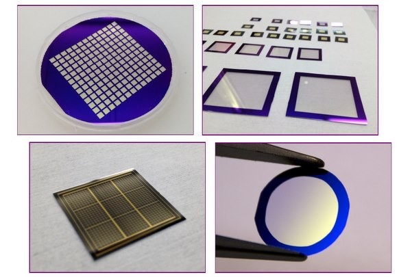
Chemical Vapor Deposition (CVD) is a cornerstone technology in the semiconductor industry, enabling the precise deposition of materials onto wafer surfaces. This process involves the transformation of gaseous raw materials into solid films through chemical reactions. The fundamental principle is that the reactants, in their gaseous state, are introduced into a reactor where they undergo a series of complex reactions. These reactions result in the formation of a new material that deposits uniformly on the substrate surface.
One of the most illustrative examples of CVD in action is the formation of a silicon nitride film (Si₃N₄). This process begins with the introduction of silane (SiH₄) and nitrogen (N₂) gases into the reactor. Under controlled temperature and pressure conditions, these gases react to form a silicon nitride film. This film is crucial in semiconductor manufacturing for its insulating properties and ability to protect underlying layers from environmental contaminants.
| Reactant | Product | Application |
|---|---|---|
| SiH₄ + N₂ | Si₃N₄ | Insulating layer, barrier |
The versatility of CVD extends beyond silicon nitride, encompassing a wide array of materials and applications. For instance, the deposition of metal films for interconnects, the creation of dielectric layers for capacitors, and the formation of protective coatings for mechanical components all rely on CVD techniques. Each application demands a tailored approach, adjusting parameters such as temperature, pressure, and gas composition to achieve the desired film properties.
In essence, CVD is not merely a deposition technique but a sophisticated process that bridges chemistry and engineering, offering solutions to the intricate challenges of modern material science and semiconductor technology.
Types of CVD Technologies
Chemical Vapor Deposition (CVD) encompasses a diverse array of processes designed to meet specific application needs. These processes include:
- Atmospheric Pressure Chemical Vapour Deposition (APCVD): Operates at atmospheric pressure, making it a cost-effective method for large-scale applications.
- Low Pressure Chemical Vapour Deposition (LPCVD): Conducted under reduced pressure, enhancing mass transfer rates and film uniformity, widely used in semiconductor manufacturing.
- Metal-Organic Chemical Vapour Deposition (MOCVD): Utilizes organic compounds and hydrides as source materials, ideal for growing a variety of semiconductor materials and heterogeneous structures.
- Plasma Assisted Chemical Vapour Deposition (PACVD) or Plasma Enhanced Chemical Vapour Deposition (PECVD): Enhances chemical activity through low-temperature plasma, enabling epitaxy at lower temperatures and improving film properties.
- Laser Chemical Vapour Deposition (LCVD): Excites chemical vapor phase reactions using laser photon energy, reducing substrate temperature and preventing damage.
- Photochemical Vapour Deposition (PCVD): Utilizes light energy to initiate chemical reactions, suitable for precise and controlled film deposition.
- Chemical Vapour Infiltration (CVI): Focuses on infiltrating porous substrates with vaporized precursor materials, commonly used in the production of ceramic composites.
- Chemical Beam Epitaxy (CBE): Employs molecular beams to deposit materials, offering high precision and control over film properties.
With technological advancements, specialized CVD technologies have emerged, each tailored for specific applications, ensuring versatility and efficiency in material science and semiconductor industries.
Advanced CVD Techniques
Plasma Enhanced Chemical Vapor Deposition (PECVD)
Plasma Enhanced Chemical Vapor Deposition (PECVD) represents a significant advancement in the field of chemical vapor deposition. Unlike conventional CVD methods, PECVD leverages the power of low-temperature plasma to significantly enhance chemical reactivity. This innovative approach allows for the deposition of high-quality films at temperatures far lower than those required by traditional techniques, typically ranging between 200-400°C. In contrast, Low Pressure Chemical Vapor Deposition (LPCVD) processes often necessitate temperatures between 425-900°C, making PECVD a more energy-efficient and substrate-friendly option.
The key to PECVD's effectiveness lies in its use of energetic electrons within the plasma, which activate the deposition process without the need for high thermal energy. This not only reduces the thermal stress on the substrate but also enables the deposition of uniform films with excellent adhesion properties. PECVD is particularly well-suited for depositing materials such as silicon nitride, amorphous silicon, and microcrystalline silicon onto a variety of substrates, including optical glass, silicon, quartz, and stainless steel.
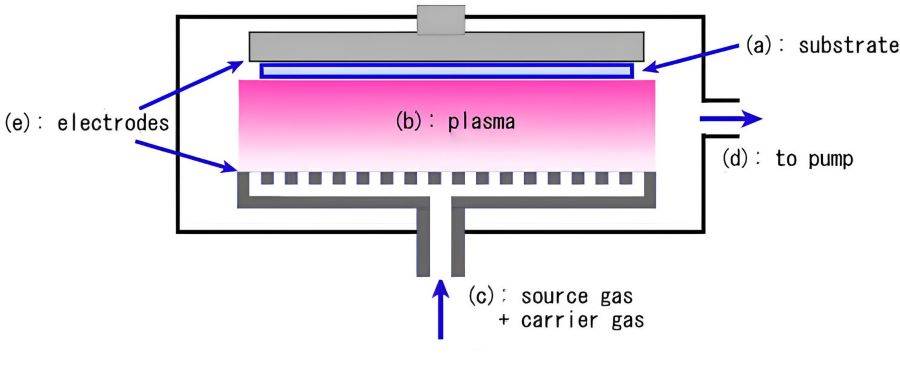
The benefits of PECVD extend beyond mere temperature reduction. The enhanced deposition rates and improved film uniformity make it an ideal choice for applications where precise control and high-quality film formation are critical. This makes PECVD a cornerstone technology in semiconductor manufacturing and material science, where the integrity and performance of deposited films are paramount.
Hot Filament Chemical Vapor Deposition (HFCVD)
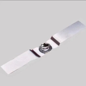
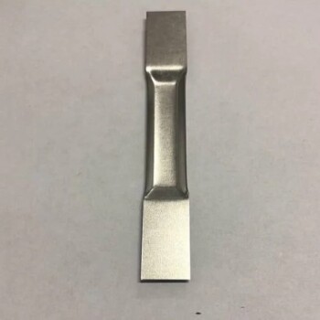
Hot Filament Chemical Vapor Deposition (HFCVD) is a specialized CVD method that operates under high-temperature and low-pressure conditions, primarily used for the production of dense films, particularly diamond films. This process involves the thermal decomposition of hydrocarbons, such as methane (CH₄), at elevated temperatures to generate the necessary precursors for film formation. The key components of an HFCVD system include a heated filament, typically made from refractory metals like tungsten (W), rhenium (Re), or tantalum (Ta), and a substrate, often made of silicon (Si).
The filament, which is maintained at temperatures ranging from 2173 to 2773 K, serves as the primary heat source, dissociating the feed gases—hydrogen (H₂) and methane (CH₄)—into smaller, reactive fragments. This dissociation occurs in the vicinity of the filament, which is positioned at a distance of approximately 2-8 mm above the pre-heated substrate, which itself is maintained at temperatures between 673 to 1373 K. The close proximity of the filament to the substrate ensures efficient heat transfer and promotes the formation of dense, high-quality films.
One of the unique aspects of HFCVD is the formation of metal carbides on the filament surface. These metal carbides act as catalysts, enhancing the dissociation of hydrogen and improving the overall efficiency of the process. However, this catalytic activity also leads to the mechanical deterioration of the filament over time. The filament can become brittle due to swelling, bending, and cracking, necessitating frequent replacements and maintenance. This mechanical degradation is a significant drawback of the HFCVD method, impacting both the process reliability and the overall cost.
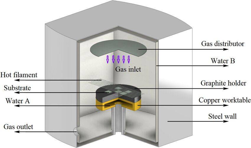
Despite these challenges, HFCVD is widely recognized for its simplicity and the relatively fast growth rates of diamond films compared to other CVD methods. The method's ability to control process conditions with ease has made it a popular choice in diamond film research and applications. However, the issue of filament brittleness and contamination remains a critical area for further research and development.
High Density Plasma Chemical Vapor Deposition (HDP-CVD)
High Density Plasma Chemical Vapor Deposition (HDP-CVD) represents a significant advancement in the realm of chemical vapor deposition techniques. Unlike conventional Plasma Enhanced Chemical Vapor Deposition (PECVD) methods, HDP-CVD employs an inductively coupled plasma (ICP) source to achieve remarkably higher plasma densities and superior quality at significantly lower deposition temperatures. This innovative approach not only enhances the efficiency of the deposition process but also significantly improves the ability to fill trenches or holes, even those with high aspect ratios, without the formation of pinch-offs or voids.
One of the standout features of HDP-CVD is its ability to provide nearly independent control over ion flux and energy. This capability is crucial for optimizing the deposition process, ensuring that the deposited material adheres well to the substrate and fills intricate structures uniformly. Moreover, the versatility of HDP-CVD extends beyond deposition; it can be seamlessly converted to Inductively Coupled Plasma Reactive Ion Etching (ICP-RIE) for plasma etching applications. This dual functionality is particularly advantageous in scenarios where budget constraints or limited system footprint necessitate a multi-functional solution.
The evolution of HDP-CVD from earlier PECVD methods underscores its technological superiority. While PECVD was effective for filling larger gaps, it struggled with smaller, high-aspect-ratio structures, often leading to defects. HDP-CVD, with its simultaneous deposition and etching capabilities, addresses these challenges head-on, making it a preferred choice for modern semiconductor fabrication processes.
In summary, HDP-CVD stands out as a cutting-edge technology in the CVD landscape, offering enhanced plasma control, improved filling capabilities, and versatile application potential, all while operating at lower temperatures. Its ability to transition between deposition and etching processes further solidifies its role as a pivotal tool in advanced semiconductor manufacturing.
Microwave Plasma Chemical Vapor Deposition (MPCVD)
Microwave Plasma Chemical Vapor Deposition (MPCVD) is renowned for its capability to produce high-quality hard films and large-size single-crystal diamonds. This method leverages electromagnetic wave energy, specifically microwave radiation, to excite reactive gases within a reactor chamber. The process initiates the formation of a pure plasma, which is a state of matter composed of a mixture of electrons, atomic ions, molecular ions, neutral atoms, molecules, and molecular fragments in their ground and excited states.
The plasma generated through MPCVD is characterized by its high electron density at the center, which gradually decreases as one moves away from the core. The primary mechanism for generating reactive gaseous precursors/fragments in the plasma is electron impact dissociation. This process involves the electrons absorbing energy from the oscillating electric field of the microwave radiation, reaching temperatures as high as 5273 K, while the gas (neutral species) temperature remains around 1073 K in low-pressure synthesis methods.
The plasma environment created by MPCVD is particularly conducive to diamond deposition. It contains reactive carbonaceous species and an excess of atomic/molecular hydrogen in the vicinity of suitable substrates, providing an ideal setting for the formation of diamond films. The most commonly used microwave frequencies for this method are 2.45 GHz and 915 MHz, which are optimized for efficient plasma generation and subsequent film deposition.
Ultra-high Vacuum Chemical Vapor Deposition (UHV/CVD)
Ultra-high Vacuum Chemical Vapor Deposition (UHV/CVD) is a sophisticated thin film technology that operates under ultra-high vacuum conditions, typically below 10^-6 Pa (10^-8 Torr). This method is particularly adept at depositing high-quality submicron crystalline films, making it indispensable for applications in nanostructured materials and silicon-based high-speed high-frequency devices.
In the UHV/CVD process, one or more volatile precursors interact with the substrate under these extreme vacuum conditions, leading to a reaction or decomposition on the substrate's surface that results in the formation of a deposit. The molecular flow achieved in this technique ensures that gas-phase chemistry is minimized, which is crucial for the deposition of chemically active single crystal thin films.
One of the standout features of UHV/CVD is its ability to produce graphene, a material known for its exceptional electrical and mechanical properties. Unlike traditional vapor phase epitaxy methods, UHV/CVD employs low-pressure and low-temperature growth conditions. This approach effectively mitigates the solid-state diffusion of doping sources and inhibits the three-dimensional growth of epitaxial films.
The ultra-high vacuum environment of the UHV/CVD reactor plays a pivotal role in preventing the oxidation of the silicon substrate surface. By minimizing the incorporation of impurities generated by the reaction gas into the growing film, UHV/CVD ensures the deposition of films with superior purity and structural integrity.
| Feature | UHV/CVD Advantage |
|---|---|
| Vacuum Level | <10^-6 Pa (10^-8 Torr) |
| Growth Conditions | Low-pressure, low-temperature |
| Film Quality | High-quality submicron crystalline films |
| Surface Protection | Prevents surface oxidation and impurity doping |
| Application | Nanostructured materials, high-speed high-frequency devices |
UHV/CVD technology, developed in the late 1980s, has since become a cornerstone in the fabrication of advanced materials and devices, particularly those requiring exceptional purity and structural precision.
Low Pressure Chemical Vapor Deposition (LPCVD)
Low Pressure Chemical Vapor Deposition (LPCVD) is a sophisticated CVD technique that operates at reduced pressures, typically around 133 Pa or less. This method significantly enhances the mass transfer rates within the reaction chamber, leading to superior film uniformity and resistivity uniformity. The low-pressure environment accelerates gas diffusion, allowing for faster transport of reactants to the substrate surface and quicker removal of impurities and by-products, thereby minimizing self-doping and boosting overall production efficiency.
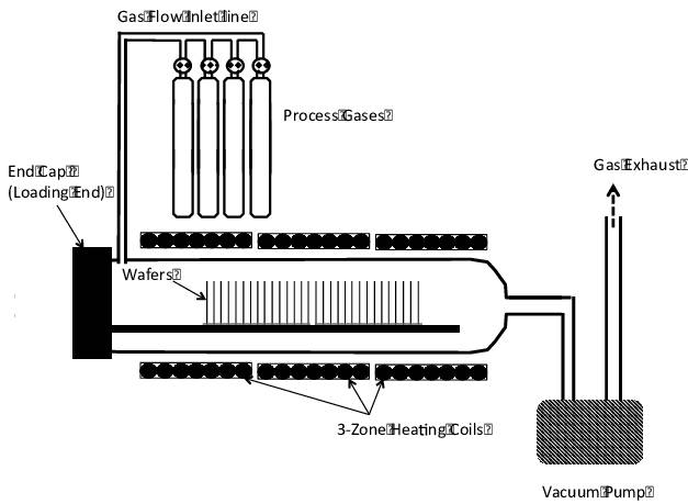
One of the key advantages of LPCVD is its ability to achieve high-quality film deposition without the need for carrier gases, which reduces the risk of particle contamination. This makes LPCVD an ideal choice for the high-value semiconductor industry, where the deposition of thin films with precise properties is critical. The technique is particularly effective for applications such as the production of resistors, capacitor dielectrics, MEMS, and anti-reflective coatings.
The operational parameters of LPCVD, including pressures ranging from 0.1 to 10 Torr and temperatures between 200 to 800°C, are meticulously controlled to ensure optimal deposition conditions. The use of a specialized precursor delivery system, often incorporating a shower head design, further enhances the precision and efficiency of the process. By cooling the shower head and chamber walls while heating the substrate, LPCVD promotes heterogeneous surface reactions, ensuring that the deposited films meet the stringent requirements of modern semiconductor manufacturing.
Thermochemical Vapor Deposition (TCVD)
Thermochemical Vapor Deposition (TCVD) is a sophisticated technique that leverages high-temperature chemical reactions to facilitate the growth of materials in the gas phase. This method is pivotal in various advanced material synthesis processes, particularly in the semiconductor industry. TCVD encompasses a range of specific techniques, each tailored to different material requirements and growth conditions.
One of the primary methods within TCVD is the chemical transport method. In this approach, the material intended for thin-film formation reacts with another solid or liquid substance in the source area, generating a gaseous compound. This gas is then transported to the growth area, where it undergoes a reverse thermal reaction, resulting in the deposition of the desired material. This method is particularly effective for creating high-quality, uniform films.
Another key technique within TCVD is the pyrolysis method. This method involves the transport of volatile substances containing the elements necessary for the film to the growth area. Once there, these substances undergo a thermal decomposition reaction, yielding the required material. The growth temperature for this process typically ranges between 1000-1050 degrees Celsius, making it suitable for applications requiring high-temperature stability and structural integrity.
TCVD also includes other methods such as synthesis reactions, which involve complex chemical interactions to produce the desired film material. Each of these methods is chosen based on the specific properties required for the final product, such as film thickness, uniformity, and adherence to the substrate.
In summary, TCVD offers a versatile toolkit for material scientists and engineers, enabling the precise control and optimization of thin-film properties through high-temperature chemical reactions. This makes TCVD an indispensable technique in the quest for advanced materials with tailored characteristics.
High Temperature Chemical Vapor Deposition (HTCVD)
High Temperature Chemical Vapor Deposition (HTCVD) is a pivotal technique for the growth of silicon carbide crystals, a material renowned for its exceptional properties such as high thermal conductivity and mechanical strength. This method operates within a closed reactor, where external heating is applied to sustain the reaction temperatures between 2000°C and 2300°C. These extreme temperatures are essential for initiating and sustaining the complex chemical reactions necessary for crystal formation.
The process of HTCVD can be broken down into several key steps:
-
Gas Introduction: A mixture of reactive gases is introduced into the reactor. These gases typically include compounds like silane (SiH₄) and propane (C₃H₈), which are essential for the formation of silicon carbide.
-
Gas Decomposition: Upon reaching the high-temperature environment, the reactive gases decompose, liberating silicon and carbon atoms. This decomposition is a critical step as it provides the elemental components required for the crystal growth.
-
Surface Reaction: The liberated silicon and carbon atoms undergo a series of surface reactions on the substrate material. These reactions result in the formation of a solid silicon carbide film. The substrate, often made of silicon or graphite, acts as a template for the crystal growth.
-
Film Growth: As the reaction proceeds, the solid silicon carbide film grows layer by layer. The continuous introduction of fresh reactive gases ensures that the growth process is sustained, allowing for the formation of thick, high-quality crystalline films.
-
Exhaust and Purge: The byproducts of the reaction, including any unreacted gases and volatile compounds, are exhausted from the reactor. This step is crucial for maintaining the purity of the growing crystal and preventing the formation of defects.
HTCVD is particularly advantageous for silicon carbide growth due to its ability to produce large, single-crystal wafers with minimal defects. This makes it an indispensable technique in industries where high-performance materials are required, such as in power electronics, aerospace, and high-temperature applications.
The success of HTCVD is rooted in its ability to manage complex thermodynamic and kinetic processes. The high temperatures not only drive the necessary chemical reactions but also enhance the diffusion of atoms on the substrate surface, leading to the formation of well-ordered crystalline structures.
In summary, HTCVD stands out as a superior method for silicon carbide crystal growth, leveraging high temperatures and precise gas management to produce materials with unparalleled properties. Its applications extend across various high-tech industries, underscoring its significance in advancing material science and technology.
Medium Temperature Chemical Vapor Deposition (MTCVD)
Medium Temperature Chemical Vapor Deposition (MTCVD) is a sophisticated process that amalgamates the principles of High Temperature Chemical Vapor Deposition (HTCVD) and MTCVD technologies to engineer super cemented carbide coating materials. This integration has proven instrumental in significantly enhancing the durability and longevity of cutting tools, particularly in high-speed and high-efficiency cutting applications.
The development of these advanced coating materials has addressed a long-standing challenge in the industry—the issue of low tool life under high-strength conditions. By leveraging the combined strengths of HTCVD and MTCVD, manufacturers have been able to create coatings that withstand the rigors of heavy cutting of alloy steel, dry cutting, and other demanding mechanical processing scenarios. This breakthrough has garnered widespread attention and is now widely adopted in the coated carbide tool industry, where its impact has been notably significant.
The MTCVD process itself operates within a specific temperature range, typically between 700 to 900°C, under controlled deposition reaction pressures of 2X10^3 to 2X10^4 Pa. The primary reaction gases, such as CH3CN, TiCl4, and H2, are carefully proportioned at a ratio of 0.01:0.02:1, and the deposition process can last from 1 to 4 hours. This meticulous control over the process parameters ensures the formation of high-quality coatings that are both durable and effective.
In summary, MTCVD represents a significant advancement in the field of chemical vapor deposition, offering a robust solution to enhance tool life in high-speed cutting applications. Its successful implementation in the industry underscores the potential for continued innovation and improvement in coating technologies.
Metal Organic Compound Chemical Vapor Deposition (MOCVD)
Metal Organic Compound Chemical Vapor Deposition (MOCVD), often referred to as Metal Organic Vapor Phase Epitaxy (MOVPE), is a sophisticated vapor phase epitaxial growth technology that has revolutionized the semiconductor industry. This technique leverages the use of organic compounds of group III and II elements, along with hydrides of group V and VI elements, as the primary source materials for crystal growth. Through the process of thermal decomposition reaction, these materials undergo vapor phase epitaxy on a substrate, facilitating the growth of various Ⅲ-V and Ⅱ-VI compound semiconductors and their multilayered solid solutions as thin single-crystal materials.
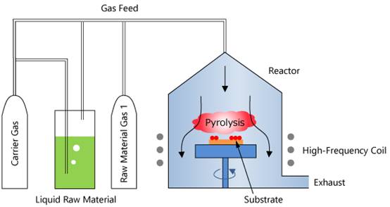
One of the standout features of MOCVD is its adaptability, making it suitable for growing a wide array of semiconductor materials and heterogeneous structures. Compared to other deposition methods, MOCVD offers higher throughput, which is a critical factor in the production of compound semiconductor devices such as High Brightness LEDs (HBLEDs). The technology's ability to control wafer carrier/slot temperature, film thickness, film stress, and wafer curvature through real-time feedback mechanisms ensures the production of high-quality films with superior performance.
In essence, MOCVD represents a significant advancement in vapor phase epitaxial growth, combining precision with efficiency to meet the stringent demands of modern semiconductor fabrication.
Laser-induced Chemical Vapor Deposition (LCVD)
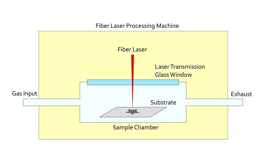
Laser-induced Chemical Vapor Deposition (LCVD) is a sophisticated technique that leverages the photon energy of a laser beam to initiate and facilitate chemical vapor phase reactions. This method is particularly advantageous as it significantly lowers the substrate temperature compared to traditional Chemical Vapor Deposition (CVD) processes. By reducing the temperature, LCVD prevents thermal damage to the substrate, making it possible to synthesize thin films on materials that are otherwise unable to withstand high temperatures.
LCVD operates through two primary mechanisms: photolytic and pyrolytic. In photolytic LCVD, the energy from the focused laser beam is absorbed by the reagent gases, causing their decomposition and subsequent deposition of solid atoms or molecules onto the substrate. This process is highly dependent on the material and typically employs UV lasers such as Ar+, ArF, and KrF.
On the other hand, pyrolytic LCVD involves the laser beam irradiating specific areas on the substrate, locally increasing the temperature to a point where gas decomposition occurs, leading to the formation of a solid layer. This method commonly uses continuous wave infrared lasers like CO2 and Nd:YAG, offering the advantage of localized heating, which can achieve finer resolutions down to 5 μm.
The LCVD system typically consists of a chamber equipped with inlets for reagent gases. The laser beam, when focused, decomposes these gases to form metallic and ceramic depositions on the substrate. The localized nature of the laser heating allows for patterning and direct writing by moving the laser beam relative to the substrate. This capability is particularly useful for creating intricate designs and structures, expanding the applications of LCVD in various industries.
In summary, LCVD stands out for its ability to deposit thin films with minimal thermal impact, offering precision and versatility in material synthesis. Its dual mechanisms of photolytic and pyrolytic processes further enhance its applicability, making it a valuable tool in both research and industrial settings.
Related Products
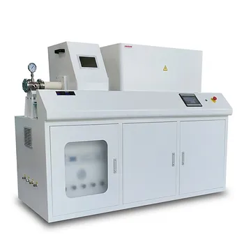
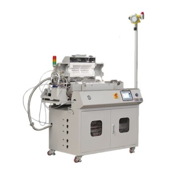
- Chemical Vapor Deposition CVD Equipment System Chamber Slide PECVD Tube Furnace with Liquid Gasifier PECVD Machine
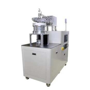
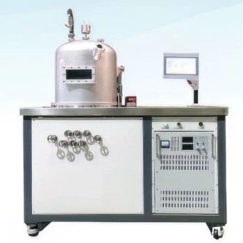
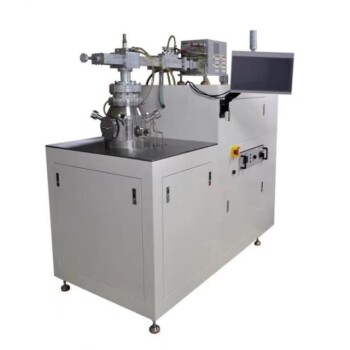
- Microwave Plasma Chemical Vapor Deposition MPCVD Machine System Reactor for Lab and Diamond Growth
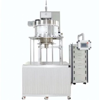
- 915MHz MPCVD Diamond Machine Microwave Plasma Chemical Vapor Deposition System Reactor
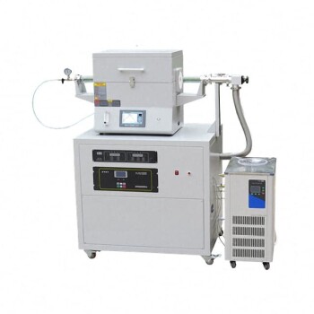
- Customer Made Versatile CVD Tube Furnace Chemical Vapor Deposition Chamber System Equipment
- Split Chamber CVD Tube Furnace with Vacuum Station Chemical Vapor Deposition System Equipment Machine
