Importance of Film Thickness
Optical Properties
The thickness of the film layer plays a pivotal role in determining the optical characteristics of materials, particularly in applications involving photonic devices and optical filters. This is because the film's thickness directly influences three key optical properties: reflection, transmission, and absorption.
- Reflection: Thicker films tend to reflect more light, which can be advantageous in applications requiring high reflectivity, such as mirrors. Conversely, thinner films reduce reflection, making them suitable for anti-reflective coatings.
- Transmission: The transmission of light through the film is inversely related to its thickness. Thicker films may block more light, while thinner films allow more light to pass through, which is crucial for transparent coatings and optical lenses.
- Absorption: The absorption of light by the film is also thickness-dependent. Thicker films can absorb more light, which is beneficial in applications like solar cells where light absorption is essential for energy conversion.
These optical properties are not merely theoretical; they have practical implications in the design and functionality of various devices. For instance, in photonic devices, precise control over film thickness is necessary to achieve desired optical responses, ensuring that the devices perform optimally under different lighting conditions. Similarly, in optical filters, the thickness of the film determines the wavelength of light that can pass through, making it a critical factor in applications ranging from camera lenses to scientific instruments.
Therefore, achieving precise film thickness tolerance is crucial for maintaining the desired optical performance, which is essential for the reliability and effectiveness of photonic devices and optical filters.
Electrical Properties
In semiconductor devices, the thickness of the film layer plays a pivotal role in determining both conductivity and insulation properties. As film thickness decreases, the risk of leakage current increases, which can adversely affect device performance and reliability. Ultra-thin films, while offering certain advantages such as increased flexibility and reduced material usage, pose significant challenges in maintaining adequate insulation.
The relationship between film thickness and electrical properties can be summarized as follows:
- Increased Conductivity with Thicker Films: Thicker films generally exhibit higher conductivity due to the increased number of conductive pathways within the material.
- Reduced Leakage Current with Thicker Films: Conversely, thicker films provide better insulation, reducing the likelihood of leakage currents that can lead to short circuits or device failures.
- Challenges with Ultra-Thin Films: Ultra-thin films, particularly those less than 10 nanometers, face the risk of increased leakage currents. This is because the insulating layer becomes so thin that it can no longer effectively block the flow of electrical charges.
To mitigate these challenges, manufacturers often employ advanced monitoring and control techniques, such as real-time monitoring using optical interferometry and X-ray reflectometry. These methods help ensure that film thickness remains within the critical tolerance levels required for optimal electrical performance.
| Film Thickness | Conductivity | Insulation Quality | Leakage Current Risk |
|---|---|---|---|
| Thick | High | Excellent | Low |
| Moderate | Moderate | Good | Moderate |
| Thin | Low | Fair | High |
| Ultra-Thin | Very Low | Poor | Very High |
In summary, while thinner films offer certain benefits, their impact on electrical properties necessitates careful control and monitoring to prevent adverse effects on semiconductor device performance.
Mechanical Properties
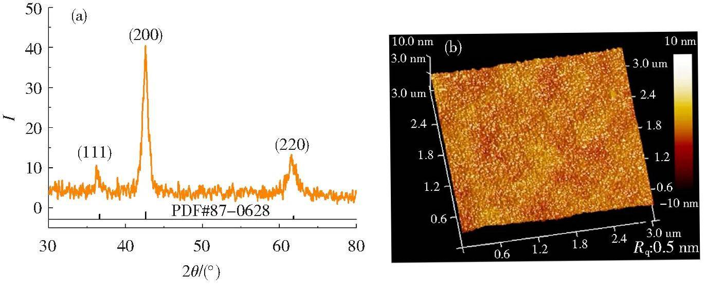
Film thickness plays a pivotal role in determining the mechanical properties of coatings, such as strength, toughness, and wear resistance. These properties are critical for enhancing the durability and longevity of the coated materials. For instance, a thicker film can provide better peel resistance, making the coating less prone to delamination or flaking under mechanical stress.
In practical applications, the mechanical properties of the film are often correlated with its thickness. A thicker film generally exhibits higher tensile strength and better resistance to abrasive wear, which are essential for applications where the coating is subject to repeated mechanical interactions. This is particularly important in industries such as automotive and aerospace, where coatings need to withstand harsh environmental conditions and mechanical stresses.
Moreover, the thickness of the film can influence its flexibility and impact resistance. Thinner films tend to be more flexible, which can be advantageous in applications requiring bending or flexing, such as in flexible electronics. However, this flexibility can come at the cost of reduced impact resistance. Conversely, thicker films offer superior impact resistance but may be less flexible, making them suitable for applications where rigidity is more critical than flexibility.
In summary, the mechanical properties of coatings are intricately linked to film thickness, and optimizing this parameter can significantly enhance the performance and durability of the coated materials in various industrial applications.
Factors Affecting Film Thickness
Source Material Nature
The characteristics of the source material play a pivotal role in determining the deposition rate during magnetron sputtering coating. Key properties such as density, melting point, and viscosity significantly influence the evaporation rate, which in turn affects the film thickness.
- Density: Higher density materials typically require more energy to vaporize, thereby affecting the rate at which particles are ejected from the target.
- Melting Point: Materials with higher melting points are more challenging to vaporize, necessitating higher sputtering power or longer processing times.
- Viscosity: The viscosity of the material affects its flow and atomization during the sputtering process, impacting the uniformity and consistency of the deposited film.
These properties collectively dictate the efficiency of the sputtering process, directly influencing the final film thickness and its uniformity.
Sputtering Parameters
Sputtering parameters are pivotal in determining the deposition rate and film thickness, which are critical for achieving the desired properties of the deposited thin films. These parameters include sputtering power, air pressure, argon flow, sputter current, sputter voltage, and vacuum pressure in the sample chamber. Each of these variables directly influences the sputter process and the quality of the coating.
For instance, sputtering power and sputter voltage are directly proportional to the energy delivered to the target material, thereby affecting the rate at which material is removed from the target and deposited onto the substrate. Higher power and voltage generally result in a higher deposition rate but may also lead to increased thermal stress on the substrate.
Air pressure and argon flow are crucial in maintaining the plasma environment necessary for sputtering. The correct balance of these parameters ensures that the ions have sufficient energy to dislodge target atoms without causing undue damage to the substrate or the coating.
Moreover, the distance between the target and the substrate plays a significant role in determining the deposition angle and efficiency. This distance affects the distribution of the sputtered material, influencing the uniformity and thickness of the deposited film.
Given the complexity of these parameters, it is often challenging to predict the exact deposition rate through theoretical calculations alone. Instead, practical measurements using thickness monitors are employed to ensure precise control over the film thickness. These monitors provide real-time data, allowing for immediate adjustments to maintain the desired film properties.
In summary, optimizing sputtering parameters is essential for achieving high-quality thin films. By carefully balancing factors such as power, pressure, and gas flow, and by utilizing advanced monitoring techniques, it is possible to control film thickness with high precision, meeting the stringent requirements of various applications.
Target-Substrate Spacing
The distance between the target and the substrate is a critical factor in magnetron sputtering, significantly influencing both the deposition angle and efficiency. This spacing directly impacts the film thickness, which in turn affects the overall quality and performance of the coating. When the target and substrate are positioned too close, the deposition angle becomes more acute, leading to non-uniform coating and potential thickness variations. Conversely, if the spacing is too wide, the efficiency of the deposition process decreases, resulting in thinner films than desired.
Optimal target-substrate spacing is essential for achieving uniform film thickness. This spacing allows for a more even distribution of the sputtered material, ensuring that the particles reach the substrate at a consistent angle and rate. By fine-tuning this distance, manufacturers can control the deposition process more effectively, leading to films with improved thickness tolerance and better performance characteristics.
For instance, in applications requiring precise optical properties, such as photonic devices and optical filters, maintaining a specific target-substrate spacing is crucial. Any deviation from the optimal distance can result in films that do not meet the required optical specifications, affecting the reflection, transmission, and absorption properties of light. Similarly, in semiconductor devices, where film thickness directly impacts conductivity and insulation properties, precise control over the target-substrate spacing is necessary to prevent issues like increased leakage current in ultra-thin films.
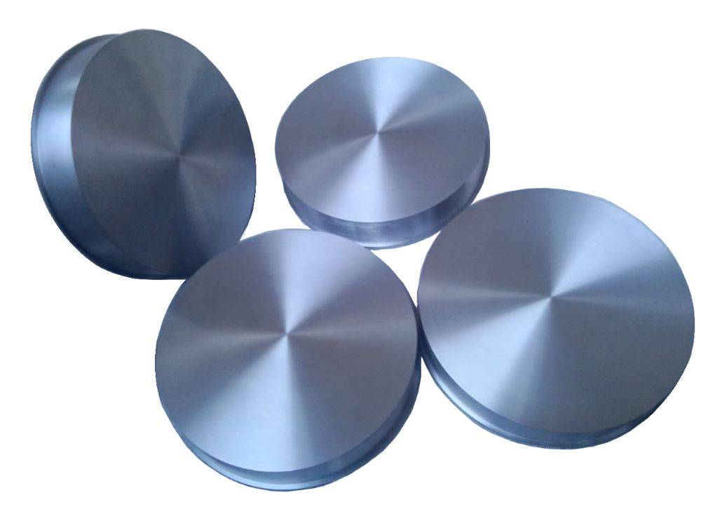
In summary, the target-substrate spacing is a pivotal parameter in magnetron sputtering that directly influences the deposition process and the resulting film thickness. By carefully managing this distance, manufacturers can achieve more uniform and high-quality coatings, meeting the stringent requirements of various applications, from optical devices to semiconductor components.
Substrate Temperature
Substrate temperature plays a pivotal role in the deposition process of magnetron sputtering coatings, significantly affecting particle migration and adhesion. When the substrate is moderately heated, it facilitates the crystallization of the deposited particles, leading to a more uniform and well-organized film structure. This controlled heating not only enhances the adhesion of the particles to the substrate but also improves the overall quality and uniformity of the coating.
The influence of substrate temperature can be further understood by examining its impact on key film properties:
- Crystallization: Moderate heating aids in the formation of crystalline structures within the film, which are crucial for enhancing the mechanical and electrical properties of the coating.
- Particle Migration: Higher substrate temperatures promote the movement of particles across the substrate surface, allowing for better distribution and reduced defects.
- Adhesion: Properly heated substrates ensure stronger adhesion between the film and the substrate, preventing delamination and improving durability.
In summary, optimizing substrate temperature is essential for achieving precise film thickness and uniformity, which are critical for the performance of coatings in various applications, from optical filters to semiconductor devices.
Target Structure and Shape
The configuration of the target, encompassing its diameter, shape, and overall design, plays a pivotal role in determining the uniformity and thickness of the coating. The geometry of the target influences the distribution of sputtered particles, which in turn affects the deposition rate and the final film characteristics.
For instance, targets with larger diameters tend to provide a more even distribution of sputtered material across the substrate, leading to enhanced coating uniformity. Conversely, targets with irregular shapes or configurations can result in non-uniform deposition, causing variations in film thickness.
| Target Feature | Impact on Coating Uniformity | Impact on Film Thickness |
|---|---|---|
| Diameter | Even distribution | Consistent thickness |
| Shape | Non-uniform distribution | Varied thickness |
| Configuration | Influences particle spread | Affects deposition rate |
Moreover, the alignment and orientation of the target relative to the substrate can also significantly impact the coating process. Proper alignment ensures that the sputtered particles reach the substrate at optimal angles, promoting uniform film growth. Misalignment, on the other hand, can lead to shadowing effects and localized thickness variations.
In summary, the meticulous design and precise positioning of the target are critical factors that directly influence the quality and consistency of the coating, ensuring that the final product meets the stringent requirements for various applications.
Monitoring and Control Methods
Real-time Monitoring Technology
Real-time monitoring of film thickness in magnetron sputtering coating processes is crucial for maintaining precise control over the final product's properties. Techniques such as scale meter measurement, optical interferometry, and X-ray reflectometry are employed to provide high-precision, real-time data on film thickness. These methods enable continuous tracking of the deposition process, allowing for immediate adjustments to ensure the film thickness remains within the desired tolerances.
-
Scale Meter Measurement: This technique uses a calibrated scale to measure the thickness of the deposited film directly. It is particularly useful for processes where the deposition rate is relatively slow and uniform.
-
Optical Interferometry: By analyzing the interference patterns created by light reflecting off the film surface, this method can determine film thickness with high accuracy. It is widely used in optical applications where precise control over film thickness is essential.
-
X-ray Reflectometry: This technique involves bombarding the film with X-rays and analyzing the reflected patterns to determine the film's thickness and density. It is particularly effective for thin films and multi-layer structures, providing detailed insights into the film's composition and uniformity.
These real-time monitoring technologies not only enhance the precision of the coating process but also facilitate the implementation of closed-loop feedback control systems, which automatically adjust sputtering parameters to maintain optimal film thickness. This integration of monitoring and control ensures that the final product meets the stringent requirements for various applications, from optical filters to semiconductor devices.

Process Control
Closed-loop feedback control systems play a pivotal role in maintaining film thickness within the desired tolerances. These systems continuously monitor the deposition process and adjust parameters in real-time to compensate for any deviations. This ensures that the film thickness remains consistent across the entire substrate, which is crucial for achieving uniform optical, electrical, and mechanical properties.
Multi-point deposition technology further enhances uniformity by distributing the deposition rate more evenly across the substrate. This method involves strategically placing multiple deposition sources around the substrate, allowing for a more controlled and uniform deposition process. By doing so, it minimizes the risk of thickness variations that could arise from localized deposition rates.
Additionally, process optimization techniques are employed to fine-tune the sputtering parameters. These techniques involve adjusting factors such as sputtering power, gas pressure, and target-substrate spacing to optimize the deposition rate and achieve the desired film thickness. This level of precision is essential for meeting the stringent tolerance standards required in applications like optical filters and semiconductor devices.
In summary, the combination of closed-loop feedback control, multi-point deposition technology, and process optimization ensures that film thickness is maintained within preset ranges, resulting in a more uniform and high-quality coating.
Tolerance Standards for Film Thickness
Optical Applications
In high-precision optical filters and reflectors, maintaining film thickness tolerance within ±5% is crucial for stable optical performance. This stringent requirement ensures that the reflection, transmission, and absorption properties of light remain consistent, which is essential for various photonic devices and optical systems.
For instance, in optical filters designed for specific wavelengths, even minor deviations in film thickness can lead to significant shifts in the filter's spectral response. This can result in erroneous data readings or reduced efficiency in applications ranging from telecommunications to medical imaging. Similarly, in reflectors, precision in film thickness is vital for achieving the desired reflectivity and minimizing losses, which is particularly important in high-energy laser systems and solar energy collectors.
To achieve this level of precision, advanced monitoring technologies such as optical interferometry and X-ray reflectometry are employed. These techniques provide real-time, high-precision measurements, allowing for immediate adjustments to maintain the film thickness within the ±5% tolerance range. Additionally, process control methods, including closed-loop feedback systems, are utilized to optimize the sputtering parameters and ensure uniformity across the entire substrate.
In summary, the optical industry demands rigorous control over film thickness to ensure the reliability and performance of optical devices. This precision not only enhances the functionality of individual components but also contributes to the overall efficiency and effectiveness of optical systems in various applications.
Electronic Devices
Ensuring semiconductor device reliability hinges on maintaining precise film thickness tolerances. Specifically, the film thickness must adhere to a stringent tolerance of ±3%. This narrow range is critical because even minor deviations can lead to significant performance issues. For instance, an overly thin film might result in increased leakage current, compromising the device's electrical integrity. Conversely, a film that is too thick could impede conductivity, affecting the overall efficiency and functionality of the semiconductor.
To achieve this level of precision, advanced monitoring and control methods are employed. Techniques such as real-time monitoring technology, including optical interferometry and X-ray reflectometry, play a pivotal role. These methods allow for continuous, high-resolution tracking of film thickness, enabling immediate adjustments to maintain the required tolerances. Additionally, process control mechanisms, such as closed-loop feedback systems, are integral in optimizing the deposition process, ensuring that the film thickness remains consistently within the ±3% range.
In practical applications, this exacting standard is exemplified in the semiconductor device growth process. Here, the combination of X-ray reflection methods with closed-loop feedback control ensures that the film thickness is maintained precisely within the ±3% tolerance. This meticulous approach not only enhances the reliability of the devices but also extends their operational lifespan, making it a cornerstone in the production of high-performance electronic components.
Decorative Applications
In decorative applications, the tolerance for film thickness can be more lenient compared to other sectors, typically allowing for variations within ±10%. This relaxed tolerance is feasible due to the primary focus on visual consistency rather than precise performance metrics like optical or electrical properties.
Visual consistency is crucial in decorative coatings, ensuring that the appearance remains uniform across different substrates and under varying lighting conditions. This is particularly important in industries such as automotive and architectural coatings, where aesthetic appeal is a key selling point. Despite the broader range of acceptable thickness variations, maintaining this visual uniformity requires careful control over the sputtering process and the use of advanced monitoring technologies.
For instance, while a ±10% tolerance might not be acceptable in optical applications, where even minor deviations can significantly alter light transmission or reflection, it is sufficient for decorative purposes. This flexibility allows manufacturers to achieve the desired visual effects without the need for ultra-precise control mechanisms, thereby reducing production costs and increasing operational efficiency.
Case Studies and Practical Experience
Film Thickness Control in Optical Filters
Achieving precise film thickness control in optical filters is paramount for maintaining optimal optical performance. These filters rely on the principle of optical interference, where the thickness of the film layers directly influences the reflection, transmission, and absorption properties of light. To ensure these properties remain consistent, real-time monitoring and adjustment techniques are employed.
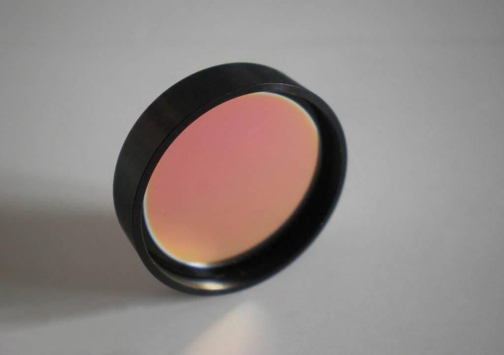
Optical interferometry stands out as a critical method for real-time film thickness monitoring in optical filters. This technique leverages the interference patterns created by light waves reflecting off the film's surface and the substrate. By analyzing these patterns, engineers can accurately determine the film's thickness and make necessary adjustments during the coating process.
| Monitoring Technique | Description | Application |
|---|---|---|
| Optical Interferometry | Uses interference patterns to measure film thickness. | High-precision optical filters. |
| X-ray Reflectometry | Measures film thickness by analyzing X-ray reflections. | Semiconductor devices. |
| Scale Meter Measurement | Mechanical measurement of film thickness. | General coating processes. |
The use of optical interferometry allows for continuous adjustments, ensuring that the film thickness remains within the stringent ±5% tolerance required for optical applications. This level of precision is essential for maintaining the filter's ability to selectively reflect or transmit specific wavelengths of light, which is crucial for applications in photonic devices and high-performance optical systems.
In addition to optical interferometry, other real-time monitoring technologies such as X-ray reflectometry and scale meter measurement are also employed to provide comprehensive data on film thickness. These technologies work in conjunction with process control systems to ensure that the coating process remains within the desired parameters, thereby maintaining the integrity and performance of the optical filters.
Semiconductor Device Growth Process
The precision of film thickness control is paramount in semiconductor device manufacturing, where even minor deviations can significantly impact device reliability. The X-ray reflection method, a sophisticated technique for real-time monitoring, plays a crucial role in this process. By measuring the interference patterns created by X-rays reflecting off the film surface, this method provides high-precision data on film thickness.
To ensure that the film thickness remains within the critical ±3% tolerance required for semiconductor devices, a closed-loop feedback control system is employed. This system continuously adjusts the sputtering parameters based on the real-time data from the X-ray reflection method. For instance, if the feedback indicates that the film is too thin, the system can increase the sputtering power or adjust the argon flow rate to compensate. Conversely, if the film is too thick, the system can reduce these parameters to bring the thickness back within the acceptable range.
This combination of advanced monitoring and precise control not only ensures the desired film thickness but also enhances the uniformity across the substrate. The result is a reliable and consistent semiconductor device performance, meeting the stringent standards necessary for modern electronic applications.
Anti-reflection Film Application
In the realm of anti-reflection films, achieving uniform film thickness is paramount for enhancing light transmission rate consistency. This uniformity is often attained through meticulous control over deposition techniques, specifically through multi-point deposition and optimizing the target-substrate distance.
Multi-point deposition involves strategically placing multiple deposition sources around the substrate. This method ensures that the film is deposited evenly across the surface, mitigating the risk of thickness variations that could lead to inconsistent optical properties. By distributing the deposition points, the process can better manage the flow of material, resulting in a more homogeneous film layer.
Simultaneously, optimizing the target-substrate distance is crucial. This distance directly influences the angle and efficiency of the deposition process. A well-calibrated distance ensures that the particles from the target material reach the substrate uniformly, thereby contributing to a more consistent film thickness. This optimization is particularly important in anti-reflection films, where even minor thickness variations can significantly impact the light transmission rate.
In summary, the combination of multi-point deposition and precise target-substrate distance optimization plays a pivotal role in achieving the uniform film thickness necessary for superior anti-reflection performance. This dual approach not only enhances the light transmission rate but also ensures the film's durability and effectiveness in various optical applications.
Related Products
- Electron Beam Evaporation Coating Oxygen-Free Copper Crucible and Evaporation Boat
- Custom PTFE Teflon Parts Manufacturer for Magnetic Stirring Bar
- Infrared Transmission Coating Sapphire Sheet Substrate Window
- Custom CVD Diamond Coating for Lab Applications
- 400-700nm Wavelength Anti Reflective AR Coating Glass
Related Articles
- Electron Beam Evaporation Coating: Principles, Characteristics, and Applications
- Crucible Types, Properties, and Applications
- The Role and Types of Crucibles in Scientific Experiments
- Understanding Evaporation Boats in Vacuum Coating
- Electron Beam Evaporation Coating Technology and Material Selection

