Introduction to Large Wafer Sizes
Market Entry and Cost Savings
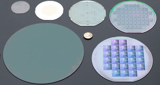
The advent of large-size wafers, ranging from 156.75 mm to 166 mm, has significantly impacted the solar cell manufacturing industry. These larger wafers, particularly the M6 type, offer substantial cost savings in both cell manufacturing and module packaging processes. One of the key advantages of M6 wafers is their comparable process times to the earlier M2 wafers, which translates to reduced manufacturing costs.
| Wafer Type | Process Time | Cost Savings |
|---|---|---|
| M2 | High | Moderate |
| M6 | Similar to M2 | Significant |
The introduction of M6 wafers not only streamlines the manufacturing process but also enhances the overall efficiency of solar cell production. This efficiency boost is critical as it directly contributes to lowering the cost per watt of solar energy, making solar power more competitive in the energy market.
Moreover, the adoption of large-size wafers aligns with industry trends towards higher efficiency and lower production costs. As new production lines in 2019 are being designed to accommodate these larger wafers, the industry is poised to see further reductions in production costs, thereby accelerating the path towards photovoltaic (PV) parity.
In summary, the market entry of large-size wafers, particularly M6, represents a pivotal shift in the solar cell manufacturing sector, offering tangible cost savings and paving the way for more efficient and cost-effective solar energy solutions.
Impact on PV Parity
The adoption of large-size cell production is a pivotal step towards achieving photovoltaic (PV) parity. The transition to larger silicon wafers, such as the M12 wafers produced by Azeus with a 210 mm edge length, significantly reduces production costs. This shift is not merely a technological upgrade but a strategic move that aligns with the industry's broader goal of cost efficiency.
New production lines introduced in 2019 are specifically designed to accommodate these larger wafers, ensuring that the equipment is compatible with the increased size. This compatibility is crucial as it allows for smoother transitions and minimizes disruptions in the manufacturing process. The M12 wafers, in particular, stand out due to their ability to further drive down production costs, making solar energy more competitive with traditional energy sources.
The cost reductions achieved through large-size wafer production are multifaceted. They include savings in material usage, enhanced efficiency in cell manufacturing, and streamlined module packaging processes. For instance, the M6 cell process times, which are comparable to those of the M2 wafers, contribute to lower manufacturing costs. This efficiency not only lowers the cost per watt but also accelerates the timeline for PV parity, where solar energy becomes cost-competitive without subsidies.
In summary, the integration of large-size wafers into the production process is a transformative development in the solar energy sector. It not only brings PV parity closer but also sets the stage for future innovations and cost reductions, ensuring that solar energy remains a viable and competitive option in the global energy market.

Challenges with Existing Equipment
Equipment Compatibility Issues
Existing equipment may face significant compatibility issues when dealing with large-sized wafers. The shift from traditional wafer sizes to larger formats, such as the M6 (166 mm) and M12 (210 mm) wafers, requires substantial technological upgrades and innovative breakthroughs. These upgrades are not merely incremental; they demand a rethinking of current manufacturing processes and equipment capabilities.
For instance, the traditional PECVD (Plasma-Enhanced Chemical Vapor Deposition) equipment, which is crucial for reducing surface reflectivity and enhancing light absorption, must be adapted to handle the larger dimensions of these wafers. This adaptation involves not only scaling up the physical size of the equipment but also optimizing the process parameters to ensure uniform coating across the expanded surface area.
Moreover, the increased size of silicon wafers necessitates modifications in supporting components such as RF power supplies, gas flow systems, and temperature control mechanisms. These changes are essential to maintain the quality and efficiency of the deposition process, which is critical for the performance of solar cells.
In summary, the transition to large-sized wafers is a complex challenge that requires comprehensive technological advancements and equipment modifications to ensure compatibility and optimal performance.
PECVD Equipment Adaptation
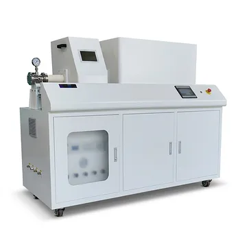
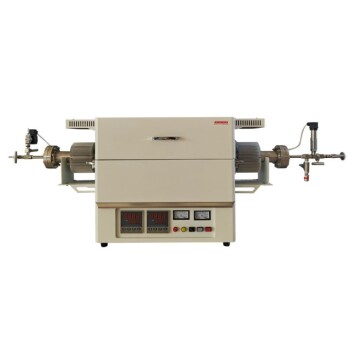
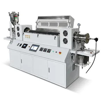
Tube PECVD equipment plays a pivotal role in the coating of M6 and M12 wafers, particularly in the context of photovoltaic cell manufacturing. This process is essential for minimizing surface reflectivity, thereby enhancing the overall light absorption efficiency of the wafers. The PECVD technique involves the deposition of thin films on the wafer surfaces, which not only reduces reflection but also improves the electrical properties of the semiconductor material.
The PECVD process begins with the substrate, typically a silicon wafer, being positioned within a deposition chamber. This chamber houses two parallel electrodes: a ground electrode and an RF-energized electrode. Precursor gases, such as silane (SiH₄) and ammonia (NH₃), are mixed with inert gases like argon (Ar) or nitrogen (N₂) to regulate the deposition process. These gases are introduced into the chamber through a showerhead fixture, ensuring an even distribution across the substrate.
Upon initiation, an electric discharge between the electrodes ignites the plasma, generating thermal energy that drives the chemical reactions necessary for film growth. High-energy electrons from the plasma collide with the precursor gas molecules, which then propagate towards the substrate. Here, they react and are absorbed onto the surface, forming the desired thin film. The byproducts of these reactions are subsequently pumped away, completing the deposition cycle.
PECVD systems are indispensable in modern semiconductor manufacturing, offering notable advantages such as excellent film uniformity, low-temperature processing capabilities, and high throughput. These systems are utilized across a broad spectrum of applications, including the fabrication of microelectronic devices, photovoltaic cells, and display panels. As the demand for advanced electronic devices continues to escalate, the significance of PECVD systems within the semiconductor industry is expected to grow even further.
PECVD Equipment Types and Advantages
Tube vs. Plate PECVD
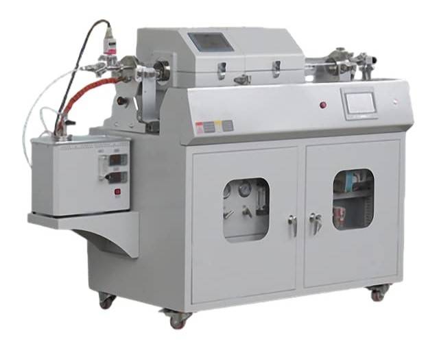
Tube PECVD stands out due to its high start-up rate, extended maintenance cycles, and superior annealing and passivation effects. This configuration is particularly favored in new production lines for the preparation of reverse passivation films. The tube setup allows for efficient gas distribution and uniform film deposition, which are critical for maintaining film density and purity, especially as thermal budgets decrease in device fabrication processes.
In contrast to furnace-driven processes, tube PECVD leverages plasma to achieve quality films at significantly lower substrate temperatures. This method not only mitigates the need for high-temperature processes but also ensures that the precursor and reactant gases are effectively dissociated within the plasma, contributing to the overall uniformity and quality of the deposited films.
The parallel-plate reactor design, common in tube PECVD, employs a powered upper electrode to generate the plasma. This setup, combined with a meticulously designed showerhead, ensures that the gases are evenly distributed across the substrate, thereby enhancing the uniformity of the deposited films. This careful configuration is pivotal for achieving the high-quality films required in modern semiconductor manufacturing.
Moreover, the preference for tube PECVD in new production lines underscores its adaptability and effectiveness in handling the increasing demands of large-sized silicon wafers. As the industry moves towards larger wafer formats to reduce production costs and enhance efficiency, tube PECVD emerges as a crucial technology for maintaining high standards in film deposition and passivation processes.
Capacity and Process Integration
The capacity of single tube PECVD systems has experienced a significant surge, enabling more efficient and scalable production processes. This increase in capacity is particularly notable in the integration of advanced processes, such as the backside 2-in-1 PECVD equipment. This innovative setup not only streamlines the production workflow but also enhances the quality of the deposited films.
One of the key advancements in this area is the integration of alumina and silicon nitride films within a single process. This integration reduces the number of steps required, thereby lowering production time and costs. The dual-film deposition process is meticulously designed to ensure that both films are applied with high precision and uniformity, crucial for maintaining the integrity and performance of the final product.
| Feature | Benefit |
|---|---|
| Increased Capacity | Allows for higher throughput, reducing production bottlenecks. |
| 2-in-1 PECVD Equipment | Simplifies the process, reducing setup and operational complexities. |
| Film Integration | Enhances film quality and consistency, crucial for device performance. |
The rapid advancements in PECVD technology are not just about increasing capacity; they are also about optimizing the process to meet the demands of large-sized silicon wafers. As the industry shifts towards larger wafer formats like M6 and M12, the need for efficient and integrated PECVD solutions becomes paramount. These advancements ensure that the equipment can handle the increased surface area and complexity of larger wafers, maintaining high standards of quality and productivity.
Specific Challenges and Solutions
Quartz Tube Size Limitations
The size of quartz tubes presents a significant constraint when loading single tubes, particularly in the context of PECVD processes designed for large-sized silicon wafers. This limitation arises because the internal dimensions of quartz tubes restrict the number of wafers that can be accommodated within a single tube. To address this challenge, several strategic solutions have been proposed.
One effective approach involves optimizing the configuration of the graphite boat, which is the carrier used to hold the wafers during the PECVD process. By reducing the number of wafers loaded per boat, it is possible to fit the wafers within the confines of the quartz tube without compromising the process efficiency. This method ensures that the wafers are adequately spaced and can be uniformly coated with the necessary films.
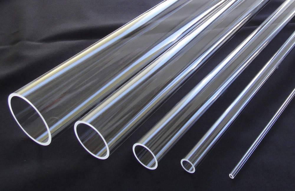
Another solution entails modifying the structure of the graphite boat itself. Innovations in boat design can facilitate better alignment and spacing of wafers, allowing for more efficient use of the available space within the quartz tube. These modifications can include changes in the boat's shape, size, or the incorporation of additional support structures to hold the wafers securely without overcrowding the tube.
| Solution | Description |
|---|---|
| Reducing Wafers per Boat | Decrease the number of wafers loaded per graphite boat to fit within the quartz tube dimensions. |
| Modifying Boat Structure | Innovate the design of the graphite boat to optimize wafer alignment and spacing within the tube. |
These adjustments not only help in overcoming the limitations imposed by quartz tube sizes but also contribute to maintaining the quality and uniformity of the PECVD coating process. By implementing these solutions, manufacturers can continue to leverage the benefits of tubular PECVD for large wafer sizes, ensuring that the equipment remains adaptable and efficient in the face of evolving technological demands.
Temperature Zone Length Limitations
As the dimensions of the graphite boat expand to accommodate larger wafers, the length of the temperature zones must also increase. This extension is crucial to ensure that the entire boat is uniformly heated, which is essential for maintaining consistent film deposition and preventing thermal gradients that could degrade the quality of the deposited layers. The longer temperature zones necessitate the introduction of additional temperature control points to manage the heating process effectively.
These control points are strategically placed along the length of the temperature zone to monitor and adjust the temperature in real-time. Each control point is equipped with sensors that provide feedback to the system, allowing for precise adjustments that ensure the temperature remains within the optimal range. This level of precision is vital for the deposition of high-quality films, which are critical for reducing surface reflectivity and enhancing light absorption in the wafers.
Moreover, the increased length of the temperature zones also impacts the overall thermal management of the PECVD system. The system must be designed to handle the additional thermal load, which can be challenging given the constraints of maintaining a uniform temperature distribution. This challenge is further compounded by the need to ensure that the temperature control points are synchronized to prevent any localized overheating or underheating that could affect the uniformity of the deposited film.
In summary, the expansion of the graphite boat dimensions to accommodate larger wafers necessitates a corresponding increase in the length of the temperature zones. This requirement drives the need for more sophisticated temperature control mechanisms, including the addition of multiple control points, to ensure the uniform heating of the entire boat and the successful deposition of high-quality films.
Supporting Component Upgrades
Upgrades to critical components such as the RF power supply, gas flow rate, and dry pumps are essential to accommodate the demands of larger wafers in tubular PECVD systems. These enhancements are pivotal for maintaining optimal performance and ensuring the uniformity of the deposition process across expanded wafer dimensions.
The RF power supply must be increased to generate higher RF currents, which are necessary to sustain the plasma discharge required for the deposition process. This increase in RF power is directly proportional to the size of the wafers, as larger wafers require more energy to maintain the same plasma density and uniformity. Additionally, the flow rate of the reactive gases must be adjusted to ensure that the gas distribution remains consistent across the surface of the larger wafers. This adjustment is crucial for achieving uniform film thickness and quality.
Moreover, the selection of dry pumps becomes more critical as the system volume increases with larger wafers. Dry pumps ensure that the vacuum environment remains stable and free of contaminants, which is essential for the high-quality deposition of thin films. The combination of these upgrades ensures that the PECVD system can handle the increased demands of larger wafers without compromising on the quality of the deposited films.

Conclusion and Future Outlook
Importance of Large Wafer Sizes
Large-size wafers are pivotal in driving down costs within the crystalline silicon cell industry. The transition from traditional wafer sizes to larger formats, such as M6 and M12, introduces a new set of challenges that necessitate a thorough reevaluation and adaptation of current manufacturing processes.
One of the primary advantages of adopting larger wafers is the potential for significant cost reductions in both cell manufacturing and module packaging. For instance, the M6 wafer, with a diameter of 166 mm, offers process times comparable to the older M2 standard, thereby reducing overall manufacturing expenses. Similarly, the M12 wafer, featuring an edge length of 210 mm, further amplifies these cost-saving benefits by optimizing material usage and minimizing waste.
However, the integration of these larger wafers into existing production lines is not without its hurdles. Equipment compatibility becomes a critical issue, as traditional machinery may not be designed to handle the increased dimensions and weight of M6 and M12 wafers. This necessitates technological upgrades and innovative solutions to ensure seamless integration and operation.
In the context of PECVD (Plasma-Enhanced Chemical Vapor Deposition) equipment, which is essential for enhancing light absorption and reducing surface reflectivity, adaptations are crucial. The tubular PECVD system, in particular, must be modified to accommodate the larger wafer sizes. This includes adjustments to the quartz tube size, temperature zone lengths, and supporting components like RF power supplies and gas flow systems.
| Challenge | Solution |
|---|---|
| Equipment Compatibility | Technological Upgrades |
| Quartz Tube Size Limitations | Modify Graphite Boat Structure |
| Temperature Zone Length Limitations | Increase Temperature Control Points |
| Supporting Component Upgrades | Enhance RF Power and Gas Flow Systems |
These adaptations not only address the immediate challenges posed by larger wafers but also pave the way for future advancements in the industry. By investing in these upgrades, manufacturers can leverage the full potential of large-size wafers, ultimately leading to more efficient and cost-effective production processes.
Industry Impact and Development
The transition to large-sized silicon wafers, such as M6 (166 mm) and M12 (210 mm), necessitates significant adaptations in equipment and processes, particularly in the realm of Plasma-Enhanced Chemical Vapor Deposition (PECVD). As the solar industry strives for cost efficiencies and higher production yields, the role of PECVD technology becomes increasingly pivotal. Tube PECVD, in particular, faces the dual challenge of enhancing its capacity while ensuring compatibility with these larger wafer formats.
To effectively serve and drive industry development, tube PECVD must undergo several critical upgrades. These include expanding the dimensions of quartz tubes to accommodate larger wafer loads, optimizing the length of temperature zones to ensure uniform coating, and enhancing the RF power supply and gas flow rates to manage the increased surface area of the wafers. Each of these modifications is essential to maintain the high standards of film quality and production efficiency that are crucial for the solar industry's ongoing advancements.
Moreover, the adoption of large wafers is not just about scaling up; it involves a comprehensive reevaluation of current manufacturing paradigms. The industry must innovate not only in equipment design but also in process integration, such as the use of backside 2-in-1 PECVD equipment that combines alumina and silicon nitride films. This integration not only streamlines the production process but also contributes to the overall cost reduction and efficiency gains that large wafers promise.
In essence, the adaptation of tube PECVD to large wafer sizes is a microcosm of the broader industry shift towards more efficient, scalable, and cost-effective solar technology. As these adaptations take hold, they will not only address immediate challenges but also pave the way for future innovations in solar energy production.
Related Products
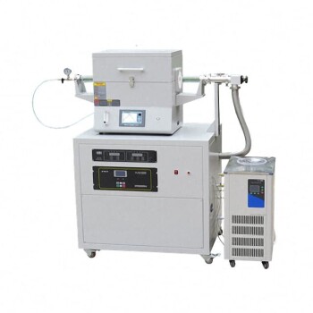
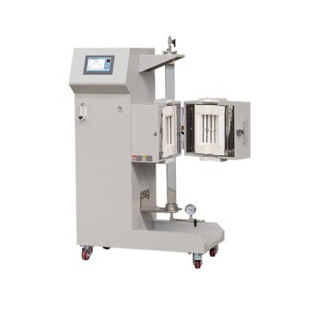
- Inclined Rotary Plasma Enhanced Chemical Vapor Deposition PECVD Equipment Tube Furnace Machine
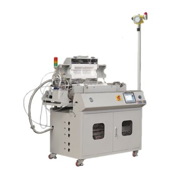
- Inclined Rotary Plasma Enhanced Chemical Vapor Deposition PECVD Equipment Tube Furnace Machine
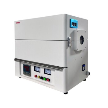
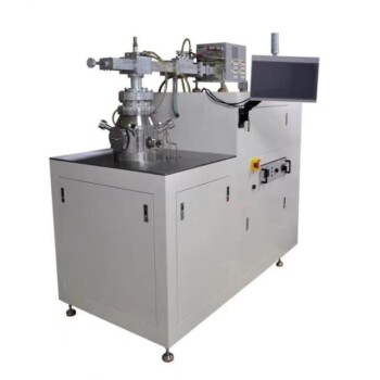
- Chemical Vapor Deposition CVD Equipment System Chamber Slide PECVD Tube Furnace with Liquid Gasifier PECVD Machine
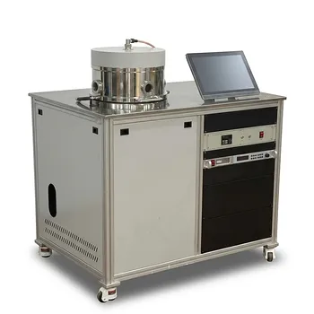
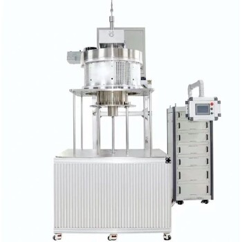
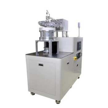
- RF PECVD System Radio Frequency Plasma-Enhanced Chemical Vapor Deposition RF PECVD
- Split Chamber CVD Tube Furnace with Vacuum Station Chemical Vapor Deposition System Equipment Machine
