Introduction to LPCVD
Definition and Importance
Low Pressure Chemical Vapor Deposition (LPCVD) stands as a cornerstone technology in semiconductor manufacturing, playing a pivotal role in the precise deposition of thin films on chip surfaces. This technique is indispensable for the fabrication of integrated circuits, ensuring that the layers applied are both uniform and of high quality. The importance of LPCVD lies in its ability to deposit various materials, such as silicon oxide, silicon nitride, and metal films, which are critical for enhancing chip performance, reliability, and functionality.
In the realm of semiconductor production, the accuracy and control offered by LPCVD are unparalleled. The process involves the introduction of gaseous precursors at low pressures, which enhances the reaction speed and homogeneity of the deposited films. This meticulous control over the chemical reactions ensures that the resulting thin films are free from defects and possess the desired electrical and mechanical properties.
Moreover, LPCVD is not limited to the deposition of insulating and protective films like silicon oxide and silicon nitride. It also extends to the introduction of impurity atoms, such as boron and phosphorus, through doping technologies. This capability is essential for modulating the conductivity of silicon, thereby influencing chip speed and power consumption. Additionally, LPCVD is employed for the deposition of conductive metal films, such as tungsten and titanium, which are vital for creating the interconnects that facilitate communication within the chip.
In summary, LPCVD is a multifaceted technology that underpins the advanced functionalities of modern semiconductors. Its ability to deliver precise, high-quality thin films and modulate material properties makes it an indispensable tool in the semiconductor industry.
Applications in Thin Film Deposition
Low Pressure Chemical Vapor Deposition (LPCVD) is pivotal in the deposition of a myriad of thin films, including silicon oxide, silicon nitride, and metal films, which are indispensable for enhancing chip performance and ensuring reliability. These films serve multiple critical functions within semiconductor devices, such as insulation, protection, and improved conductance.
The versatility of LPCVD extends beyond semiconductors to various other applications. For instance, in the optical industry, LPCVD is utilized to create coatings that enhance properties like transmission, refraction, and reflection. This technology is behind the ultraviolet (UV) filters in prescription glasses and the anti-reflective glass used in framed photos. Additionally, ceramic thin films produced via LPCVD exhibit anti-corrosive, hard, and insulating properties, making them ideal for use in sensors, integrated circuitry, and more complex designs.
Moreover, the ability of LPCVD to deposit ultra-small, "intelligent" structures opens up new frontiers in technology. This includes the development of advanced components such as batteries, solar cells, drug delivery systems, and even quantum computers. The precision and control offered by LPCVD ensure that these structures are both functional and durable, pushing the boundaries of what is possible in modern technology.
In summary, LPCVD's role in thin film deposition is not limited to semiconductor manufacturing but spans across multiple industries, contributing to the development of innovative and high-performance materials and devices.
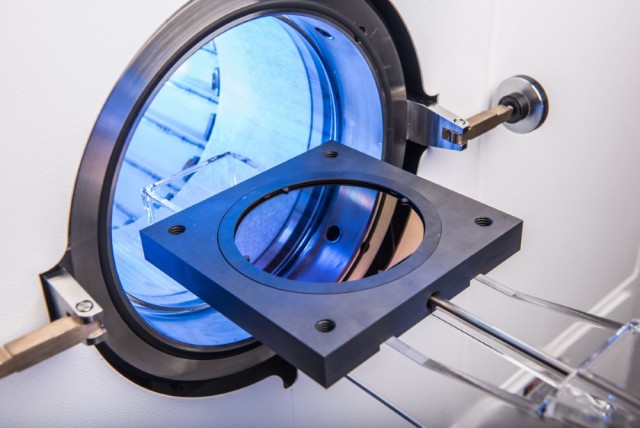
LPCVD Technology
Silicon Oxide and Silicon Nitride Films
Low Pressure Chemical Vapor Deposition (LPCVD) is renowned for its ability to produce high-quality silicon oxide (SiO₂) and silicon nitride (Si₃N₄) films, which are indispensable for insulation and protection in semiconductor chips. These films are not only crucial for their dielectric properties but also for their robust mechanical and chemical characteristics.
Silicon nitride films, in particular, have garnered significant attention due to their versatile applications in both electronic and optical systems. These amorphous films exhibit exceptional adhesion to silicon (Si) and silicon dioxide (SiO₂), making them an excellent choice as diffusion barriers against water molecules and sodium ions—two primary sources of corrosion and instability in microelectronics. This property is further enhanced by their high chemical stability and inertness, which are vital for the design of reliable biochemical and biomedical devices.
Moreover, the mechanical properties of silicon nitride films are noteworthy. They possess high values of hardness (~19 GPa) and Young’s modulus (~150 GPa), which are approximately 2–5 and 3 times higher than those of silicon dioxide, respectively. These attributes contribute to their durability and resistance against mechanical stresses, making them ideal for protective coatings in integrated circuits.
In the optical domain, silicon nitride films offer a high refractive index that can be tailored to match various applications, ranging from that of silicon nitride (nD = 2) to amorphous silicon (nD = 3.5). This tunability, combined with their low optical absorption in the visible and infrared spectral ranges, makes them suitable for a myriad of optical applications, including antireflective coatings for silicon solar cells, fabrication of optical waveguides, and the design of novel photonic and optoelectronic devices.
The properties of silicon nitride films are also highly dependent on the deposition conditions, particularly in techniques like Plasma Enhanced Chemical Vapor Deposition (PECVD). PECVD offers the advantage of low deposition temperatures (<400°C), resulting in films with minimal pinhole density, excellent uniformity, and superior step coverage. These characteristics make PECVD-deposited silicon nitride films a preferred choice for the final protective layer in integrated circuits, as well as for applications requiring wear-resistant and corrosion-resistant coatings, surface passivation, interlayer insulation, and dielectric capacitance.
Doping Technology
Low Pressure Chemical Vapor Deposition (LPCVD) plays a pivotal role in semiconductor manufacturing by introducing impurity atoms such as boron and phosphorus into the silicon substrate. This process, known as doping, is essential for modulating the electrical conductivity of silicon, thereby influencing critical parameters like chip speed and power consumption.
Doping with boron enhances the p-type conductivity, while phosphorus promotes n-type conductivity. These adjustments are crucial for creating the necessary electronic properties within semiconductor devices, enabling features such as transistors and diodes. The precise control of doping levels ensures that the resulting chips can operate efficiently under varying conditions, optimizing both performance and energy usage.
Moreover, the uniformity and precision of LPCVD doping techniques are paramount. Any variability in the doping process can lead to inconsistencies in chip performance, affecting the overall reliability and yield of semiconductor production. Thus, LPCVD's ability to deliver homogeneous doping distributions across large wafers is a significant advantage, particularly in the context of modern high-density integrated circuits.
In summary, LPCVD's doping technology is not merely an additive process but a fundamental aspect of semiconductor engineering, directly impacting the functionality and efficiency of the final electronic products.
Metal Film Deposition
Low Pressure Chemical Vapor Deposition (LPCVD) plays a pivotal role in depositing metal films such as tungsten and titanium, which serve as critical conductive channels for chip interconnects. This process involves the use of charged ions, often in the form of electron beams, which bombard the substrate material within a vacuum chamber. As the electron beams evaporate the source material, it solidifies into a thin metal coating on the substrate surface, ensuring precise and uniform deposition.
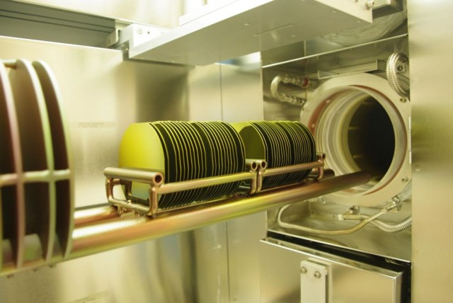
The applications of thin metal film deposition are vast and varied, spanning across semiconductor manufacturing, fiberoptic systems, industrial laser systems, medical electronics, and advanced optical and imaging applications. In semiconductor fabrication, these metal films are indispensable for enhancing the conductivity and reliability of integrated circuits. The electron beam evaporation technique, in particular, offers a versatile solution for depositing both metal and dielectric materials, making it suitable for a range of applications including lift-off processes, ohmic contacts, insulation, and optical coatings.
One of the key advantages of LPCVD in metal film deposition is its ability to maintain a low chamber pressure, which minimizes the risk of chemical reactions between the background gases and the film process. This controlled environment ensures the integrity and high quality of the deposited metal films, which are essential for the performance and longevity of electronic devices.
LPCVD Operation Principles
Chemical Reaction Control
In the realm of Low Pressure Chemical Vapor Deposition (LPCVD), the meticulous orchestration of chemical reactions is paramount. This process hinges on the precise management of five critical phases: gas delivery, adsorption, reaction, deposition, and residual gas removal. Each step is intricately linked, ensuring the successful formation of high-quality thin films essential for semiconductor devices.
The gas delivery phase involves the introduction of gaseous precursors into the reaction chamber at low pressure. This low-pressure environment is crucial as it enhances the speed and homogeneity of the reactions, minimizing the likelihood of unwanted side reactions and ensuring uniform film deposition.
Following gas delivery, the precursor molecules adsorb onto the substrate's surface. This adsorption process is a delicate balance, where the molecules must attach to the substrate without forming clusters that could disrupt the uniformity of the film.
Once adsorbed, the precursor molecules undergo chemical reactions to form new compounds. These reactions are carefully controlled to ensure the desired film properties, such as thickness, density, and composition, are achieved. The deposition phase then follows, where the reaction products settle onto the substrate, forming the thin film.
Finally, the residual gas removal phase is essential for maintaining process stability. Unreacted gases and by-products are purged from the chamber to prevent contamination and ensure the purity of the deposited film. This meticulous control over each step guarantees the production of high-quality thin films that are integral to the performance and reliability of semiconductor devices.
Gas Transportation
In the realm of Low Pressure Chemical Vapor Deposition (LPCVD), the efficient transportation of gaseous precursors is a critical aspect that directly influences the quality and homogeneity of the deposited films. These precursors, typically introduced at pressures significantly lower than atmospheric, play a pivotal role in enhancing both the speed and uniformity of the chemical reactions occurring on the substrate surface.
The low-pressure environment within the LPCVD chamber is meticulously controlled to ensure that the gaseous precursors can diffuse more freely and uniformly across the substrate. This diffusion is crucial as it minimizes the likelihood of reaction hotspots, thereby promoting a more consistent film thickness and composition. The reduced pressure not only accelerates the reaction kinetics but also facilitates the removal of by-products and unreacted gases, maintaining the cleanliness and integrity of the deposition process.
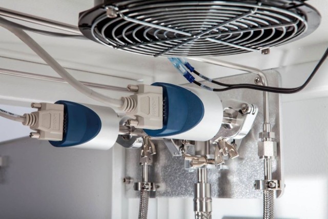
To further illustrate the importance of gas transportation in LPCVD, consider the following key points:
-
Pressure Control: The pressure within the LPCVD chamber is typically maintained in the range of 0.1 to 10 Torr. This low pressure regime allows for efficient gas diffusion and minimizes the mean free path of gas molecules, ensuring they reach the substrate uniformly.
-
Gas Flow Management: Precise control of gas flow rates is essential. This involves the use of mass flow controllers (MFCs) to meter the introduction of precursors, ensuring optimal concentrations are maintained for the desired chemical reactions.
-
Mixing and Homogeneity: Proper mixing of the gaseous precursors is achieved through the design of the LPCVD reactor. Techniques such as laminar flow and the use of baffles help in achieving a homogeneous distribution of gases, which is vital for uniform film deposition.
By meticulously managing the transportation and distribution of gaseous precursors, LPCVD processes can achieve the high levels of precision and consistency required for modern semiconductor manufacturing.
Adsorption and Reaction
During the Low Pressure Chemical Vapor Deposition (LPCVD) process, the precursor molecules, which are typically gaseous compounds, are introduced into the reaction chamber at low pressure. These molecules then migrate towards the substrate, which is the surface where the thin film will be deposited. Upon reaching the substrate, the precursor molecules adsorb onto its surface, adhering through weak van der Waals forces or stronger chemical bonds, depending on the nature of the precursor and the substrate material.
Once adsorbed, these precursor molecules undergo a series of complex chemical reactions. These reactions can involve breaking and forming bonds, resulting in the transformation of the precursor molecules into new compounds that are integral to the thin film's composition. For instance, in the deposition of silicon oxide (SiO₂) or silicon nitride (Si₃N₄) films, the precursor molecules react with the substrate or with each other to form the desired compounds.
The reactions that occur during adsorption are highly dependent on the temperature and pressure within the reaction chamber. Typically, higher temperatures facilitate more rapid and complete reactions, while low pressure helps to ensure uniform distribution of the precursor molecules and the reaction products. This controlled environment is crucial for the quality and consistency of the deposited film.
Additionally, the nature of the substrate can influence the adsorption and reaction processes. For example, a substrate with a high surface energy may attract and hold precursor molecules more effectively, promoting more efficient reactions. Conversely, a substrate with a low surface energy might require more precursor molecules or additional surface treatments to achieve the same level of film deposition.
In summary, the adsorption and reaction steps in LPCVD are fundamental to the formation of high-quality thin films. By carefully managing the conditions within the reaction chamber, manufacturers can optimize these processes to achieve the desired film properties, which are essential for the performance and reliability of semiconductor devices.
Deposition and Gas Removal
In the Low Pressure Chemical Vapor Deposition (LPCVD) process, the formation of thin films on the substrate is a critical step. This process involves several intricate phases, starting with the introduction of gaseous precursors, their adsorption onto the substrate, and subsequent chemical reactions that lead to the deposition of reaction products. The deposition itself is a meticulously controlled event, where the newly formed compounds settle uniformly on the substrate surface, ensuring the desired film thickness and properties.
However, the process is not complete without the removal of unreacted gases and by-products. These residual gases, if not effectively managed, can lead to defects in the deposited film, compromising the overall quality and stability of the semiconductor device. Therefore, a robust gas removal system is essential to maintain the integrity of the LPCVD process. This system typically involves the use of vacuum pumps and scrubbers that efficiently extract the unreacted gases, ensuring that the deposition environment remains stable and conducive to high-quality film formation.
The importance of effective gas removal cannot be overstated, as it directly impacts the uniformity and consistency of the deposited films. By maintaining a clean and controlled environment, the LPCVD process can achieve the precise thin film deposition necessary for advanced semiconductor manufacturing, contributing to the performance and reliability of the final chip products.
LPCVD Machine Types
Vertical LPCVD
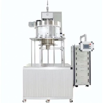
Vertical Low Pressure Chemical Vapor Deposition (LPCVD) systems are renowned for their exceptional uniformity and productivity, making them ideal for large-scale semiconductor manufacturing. These systems operate under subatmospheric pressures, allowing for precise control of temperature and gas flow, which are critical for achieving high-quality thin film deposition. The vertical configuration of these systems ensures that the growth rate is primarily limited by the surface reaction, which is highly temperature-dependent. This configuration also facilitates excellent within-wafer, wafer-to-wafer, and run-to-run uniformities, which are crucial for maintaining consistent product quality.
The vertical orientation of LPCVD systems is particularly advantageous for large-scale production due to its ability to handle multiple wafers simultaneously, thereby increasing throughput. This design minimizes the risk of nonuniform film removal, which can occur in systems that operate at extremely high temperatures. By maintaining optimal process conditions, vertical LPCVD systems can achieve a balance between high throughput and superior film quality, making them indispensable in modern semiconductor fabrication.
Moreover, the precision control over the LPCVD process, including gas delivery, adsorption, reaction, deposition, and residual gas removal, ensures that the deposited films meet the stringent requirements of semiconductor manufacturing. This level of control is essential for the production of high-performance chips that are used in a wide range of electronic devices. The ability to deposit various thin films, such as silicon oxide, silicon nitride, and metal films, further underscores the versatility and importance of vertical LPCVD systems in the semiconductor industry.
Horizontal LPCVD
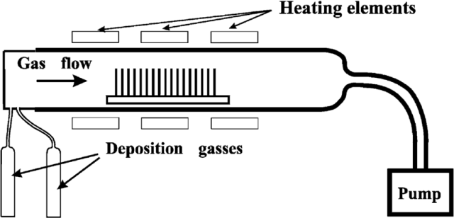
Horizontal Low Pressure Chemical Vapor Deposition (LPCVD) systems stand out for their simplicity and cost-effectiveness, making them ideal for small-scale research and development (R&D) or specialized applications. Unlike their vertical counterparts, which are optimized for large-scale production, horizontal LPCVD systems are designed to be more adaptable and less complex. This adaptability is particularly beneficial in scenarios where flexibility and rapid prototyping are crucial.
The horizontal configuration of these systems enhances the gas diffusion coefficient and mean free path within the reaction chamber. This improvement significantly boosts film uniformity, resistivity uniformity, and trench coverage filling capability. The low pressure environment not only accelerates the gas transport rate but also facilitates the quick removal of impurities and reaction by-products, thereby minimizing self-doping and enhancing overall production efficiency.
Moreover, horizontal LPCVD systems do not require carrier gases, which significantly reduces the risk of particle contamination. This makes them particularly attractive for use in high-value semiconductor manufacturing, where the deposition of pristine thin films is paramount. The absence of carrier gases also translates to lower operational costs and a smaller environmental footprint, further contributing to their cost-effectiveness.
In summary, horizontal LPCVD systems offer a balanced mix of efficiency, flexibility, and cost-effectiveness, making them a preferred choice for R&D environments and specialized manufacturing needs. Their unique design features ensure high-quality film deposition while maintaining a streamlined and economical operation.
Future of LPCVD
Technological Innovations
Continuous advancements in equipment design and process parameters are pivotal in refining the precision and efficiency of Low Pressure Chemical Vapor Deposition (LPCVD) systems. These innovations are not merely incremental but are transformative, aiming to push the boundaries of what is possible in semiconductor manufacturing.
One of the key areas of focus is the optimization of reactor geometries. Traditional vertical and horizontal LPCVD systems are being reimagined with novel designs that enhance gas flow uniformity and reduce dead zones within the reactor. This ensures that every wafer receives a consistent layer of deposition, thereby improving the overall yield and quality of the semiconductor devices.
In parallel, there is a concerted effort to integrate advanced automation and control systems. These systems leverage artificial intelligence and machine learning algorithms to dynamically adjust process parameters in real-time. For instance, AI-driven predictive models can anticipate and mitigate potential process deviations, ensuring that the deposition process remains stable and within the desired specifications.
Moreover, the development of new materials and precursors is revolutionizing LPCVD. Traditional silicon-based films are being complemented by novel materials such as two-dimensional materials and high-k dielectrics. These materials offer superior electrical and thermal properties, enabling the creation of more efficient and powerful semiconductor devices.
The synergy between these technological advancements is driving the future of LPCVD, making it not only a cornerstone of current semiconductor manufacturing but also a key enabler for the next generation of electronic devices.
New Applications
LPCVD is not only advancing in traditional semiconductor materials but is also venturing into cutting-edge realms, particularly with the integration of two-dimensional materials and high-k dielectrics. These new materials present unique challenges and opportunities, pushing the boundaries of what LPCVD can achieve.
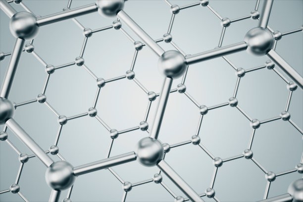
Two-Dimensional Materials
The exploration of two-dimensional materials, such as graphene and transition metal dichalcogenides (TMDs), is revolutionizing the semiconductor industry. These materials offer exceptional electrical and thermal properties, making them ideal for next-generation devices. LPCVD's precise control over thin film deposition is crucial for the uniform and defect-free layering of these materials, which are often only a few atoms thick. This capability ensures that the intricate structures required for advanced transistors and sensors can be fabricated with high fidelity.
High-k Dielectrics
High-k dielectrics, materials with a high dielectric constant, are essential for improving the performance and energy efficiency of modern transistors. LPCVD's ability to deposit these materials with high uniformity and low defect density is pivotal for their effective integration into semiconductor devices. By using LPCVD, manufacturers can achieve the necessary thin, yet robust, dielectric layers that enhance gate insulation and reduce leakage currents. This is particularly important as transistors continue to shrink, demanding materials with superior dielectric properties.
In summary, LPCVD's expansion into these new materials not only demonstrates its versatility but also positions it as a key enabler for future semiconductor innovations.
Related Products
- Inclined Rotary Plasma Enhanced Chemical Vapor Deposition PECVD Equipment Tube Furnace Machine
- RF PECVD System Radio Frequency Plasma-Enhanced Chemical Vapor Deposition RF PECVD
- Inclined Rotary Plasma Enhanced Chemical Vapor Deposition PECVD Equipment Tube Furnace Machine
- Microwave Plasma Chemical Vapor Deposition MPCVD Machine System Reactor for Lab and Diamond Growth
- Chemical Vapor Deposition CVD Equipment System Chamber Slide PECVD Tube Furnace with Liquid Gasifier PECVD Machine

