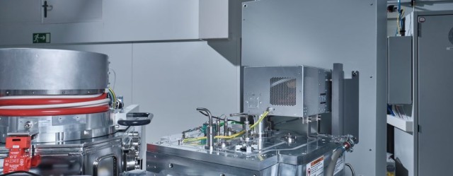
Introduction to PECVD
Overview of PECVD
PECVD (Plasma Enhanced Chemical Vapor Deposition) is a sophisticated thin film deposition technique that is extensively utilized in the semiconductor industry. This method synergistically combines the foundational principles of chemical vapor deposition (CVD) with advanced plasma technology, enabling the production of high-quality films with meticulously controlled properties. Unlike traditional CVD processes, PECVD leverages plasma to intensify the deposition process, facilitating the deposition of more material at significantly lower temperatures.
The integration of plasma into the CVD process confers several advantages. PECVD-deposited films exhibit superior physical properties, including uniformity, high cross-linking, and robust resistance to chemical and thermal changes. These attributes render PECVD-deposited films ideal for a myriad of applications, particularly in optical coatings and dielectric films. The low cost and high efficiency of plasma-applied polymers have expanded the scope of PECVD applications, making it a cornerstone technology in modern manufacturing.
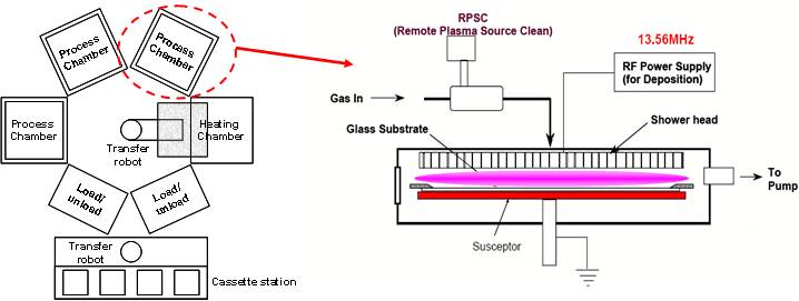
PECVD offers unparalleled control over material properties such as stress, refractive index, and hardness. This precision is crucial for producing films used in semiconductor devices for encapsulation, surface passivation, and conductive layer isolation. The technology operates by generating a low-temperature plasma within a process chamber, which induces a glow discharge at the cathode. This discharge, coupled with the introduction of process gases, triggers a series of chemical and plasma reactions that culminate in the formation of a solid film on the sample surface.
In essence, PECVD stands out as a versatile and efficient deposition technique, capable of producing high-quality films at lower temperatures, thereby preserving the integrity of delicate semiconductor structures. Its ability to control and tailor material properties makes it an indispensable tool in the semiconductor industry and beyond.
Versatility of PECVD
Plasma Enhanced Chemical Vapor Deposition (PECVD) stands out as a highly adaptable manufacturing technique, leveraging plasma to augment the reactivity of both organic and inorganic chemical precursors. This enhanced reactivity broadens the spectrum of materials that can be used as precursors, even including those that are typically inert. PECVD's capability to handle precursors in solid, liquid, or gaseous forms facilitates rapid, solvent-free fabrication of thin film coatings.
PECVD's versatility extends beyond just material diversity. The technique excels in controlling various material properties such as stress, refractive index, and hardness, making it a preferred method for applications in the semiconductor industry. For instance, PECVD is instrumental in device encapsulation, surface passivation, and conductive layer isolation. The uniformity and cross-linked nature of PECVD-deposited films contribute to their excellent physical properties, including resistance to chemical and thermal changes.
Moreover, PECVD's flexibility in adjusting film compositions allows for the creation of organic films with tailored chemical, thermal, optical, electrical, and mechanical properties. This adaptability is particularly valuable in large-scale applications on substrates like glass and silicon. Recent advancements have also seen PECVD being employed in biological applications, such as medical device protection, and in mitigating corrosion in optical and dielectric devices.
Principles of PECVD
Plasma Generation Methods
Plasma in a PECVD (Plasma Enhanced Chemical Vapor Deposition) process is typically generated by applying a voltage to electrodes embedded in a low-pressure gas environment. This voltage creates an electric field that ionizes the gas molecules, initiating the formation of plasma. The generation methods vary depending on the type of power supply used, which includes Radio Frequency (RF), Medium Frequency (MF), pulsed DC, and direct DC.
-
Radio Frequency (RF) Plasma: This method uses an alternating current with a frequency in the range of 13.56 MHz. RF plasma is widely used due to its ability to generate a stable and uniform plasma, which is crucial for high-quality film deposition.
-
Medium Frequency (MF) Plasma: Operating at frequencies between RF and DC, MF plasma offers a balance between the stability of RF and the simplicity of DC. It is particularly useful for applications requiring moderate plasma density.
-
Pulsed DC Plasma: This method involves applying a series of short pulses of direct current to the electrodes. The pulsing allows for precise control over the plasma density and energy, which can be beneficial for certain material deposition processes.
-
Direct Current (DC) Plasma: Using a continuous direct current, DC plasma is simpler to implement but less stable compared to RF and MF plasmas. It is often used in applications where lower plasma densities are acceptable.
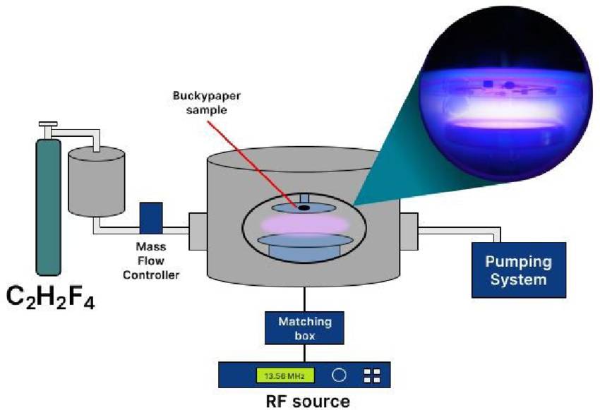
The energy provided by these power sources activates the gas or vapor, causing it to dissociate into electrons, ions, and neutral radicals. These charged and neutral particles are essential for the chemical reactions that lead to the deposition of thin films. The choice of plasma generation method depends on the specific requirements of the deposition process, such as the desired film properties, deposition rate, and substrate sensitivity to temperature.
Deposition Process
PECVD technology leverages low-temperature plasma to initiate a glow discharge at the cathode within the deposition chamber, operating under a low gas pressure environment. This glow discharge, or alternative heating mechanisms, elevates the sample temperature to a pre-set level. Subsequently, a meticulously controlled quantity of process gas is introduced into the chamber. This gas undergoes a series of intricate chemical and plasma reactions, culminating in the formation of a solid film on the sample's surface.
The deposition process is a critical phase in PECVD, where the properties of the final film are determined. The thickness of the deposited layer can vary significantly, ranging from a single atom's width (nanometer scale) to several millimeters, depending on the specific coating method and the type of material being deposited. This flexibility allows for the creation of both thin, functional coatings and thicker, protective layers, broadening the applicability of PECVD across various industries.
Key to the success of the deposition process are the precise control and optimization of several parameters, including gas flow rates, plasma power, and chamber pressure. These parameters collectively influence the mean free path of the reactants, the surface mobility of these reactants, and ultimately, the composition and properties of the deposited film. By fine-tuning these variables, it is possible to achieve films with desired characteristics such as high uniformity, specific electrical properties, or enhanced mechanical strength.
The versatility of PECVD in handling a wide array of precursor materials—whether in solid, liquid, or gaseous form—further enhances its utility. This capability ensures that PECVD can be adapted to meet the diverse needs of different applications, from semiconductor manufacturing to biomedical device production. The ability to deposit a variety of materials, including silicon nitride, silicon dioxide, amorphous silicon, and diamond-like carbon, underscores the broad spectrum of possibilities that PECVD offers.
Materials Deposited Using PECVD
Silicon Nitride (SiN)
Silicon Nitride (SiN) is a high-performance advanced ceramic material that stands out for its exceptional combination of mechanical, thermal, and electrical properties. As a material deposited via PECVD (Plasma Enhanced Chemical Vapor Deposition), SiN is renowned for its excellent dielectric properties, high thermal stability, and low conductivity. These attributes make it a preferred choice for a variety of critical applications.
In the realm of semiconductor devices, SiN is employed not only for its dielectric properties but also for its ability to serve as an effective diffusion barrier against water molecules and sodium ions, which are primary sources of corrosion and instability in microelectronics. This dual functionality ensures the longevity and reliability of semiconductor components.
Beyond semiconductors, SiN finds extensive use in biomedical devices. Its chemical stability and inertness are paramount in the design of reliable biochemical and biomedical devices, where material compatibility with living tissues is crucial. The material's high hardness (~19 GPa) and Young’s modulus (~150 GPa) further enhance its applicability in these sensitive environments, providing durability without compromising biocompatibility.
In optical coatings, SiN's high refractive index, which can be tailored to match specific requirements, makes it an ideal candidate for antireflective coatings and protective layers. Its low optical absorption across the visible and infrared spectrum allows for the fabrication of high-performance optical waveguides and planar optical systems, contributing to the advancement of photonic and optoelectronic devices.
Furthermore, SiN's high thermal shock and impact resistance, coupled with its superior creep and oxidation resistance, make it a robust material for high-temperature and high-load applications. This versatility ensures that SiN can withstand the most demanding industrial conditions, solidifying its position as a material of choice in various high-stakes industries.
Silicon Dioxide (SiO2)
Silicon dioxide, commonly referred to as silica, is a versatile material with the chemical formula SiO2. It is one of the most frequently deposited materials in Plasma Enhanced Chemical Vapor Deposition (PECVD) processes due to its exceptional dielectric properties and transparency. This oxide of silicon is most notably found in nature as quartz and is a key component in various living organisms.
In industrial applications, silicon dioxide is often used in its fused quartz form, which is renowned for its high purity and unique physical properties. Notably, silicon dioxide is a major constituent of sand in many parts of the world, making it abundantly available for industrial use. The material is not only used in semiconductor manufacturing but also finds applications in optical coatings, structural materials, and as a protective layer against corrosion and for enhancing hydrophobicity.
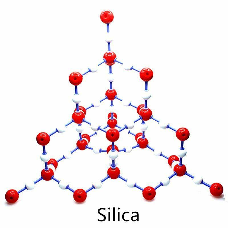
Silicon dioxide's role in microelectronics is particularly significant. As an electrical insulator, it ensures the proper functioning of semiconductor devices by preventing short circuits and maintaining signal integrity. Its use extends beyond electronics to the food and pharmaceutical industries, where it serves as a critical component in various formulations and processes.
The deposition of silicon dioxide using PECVD allows for precise control over the film's properties, enabling tailored solutions for specific applications. Whether in the form of fused quartz, fumed silica, silica gel, or aerogels, silicon dioxide continues to be a cornerstone material in modern technology, underscoring its importance in both current and emerging applications.
Amorphous Silicon (a-Si)
Amorphous silicon, often abbreviated as a-Si, stands out as a non-crystalline form of silicon with distinct electronic properties. Unlike its crystalline counterpart, a-Si lacks a well-defined crystal structure, which imparts it with unique optical and electrical characteristics. This material is particularly renowned for its application in thin-film technology, where its ability to be deposited in layers as thin as a few nanometers is highly advantageous.
One of the most significant applications of a-Si lies in the production of thin-film solar cells. These solar cells leverage the photovoltaic effect to convert sunlight into electricity, and a-Si's ability to absorb a broad spectrum of light makes it an ideal candidate for this purpose. Additionally, the material's low production costs and compatibility with flexible substrates further enhance its appeal in the renewable energy sector.
Beyond solar cells, a-Si finds extensive use in the fabrication of photodetectors and display devices. In photodetectors, a-Si's sensitivity to light allows it to detect and measure light intensities with high precision, making it indispensable in various optical sensing applications. In display technology, a-Si is utilized in the construction of thin-film transistors (TFTs), which are crucial components in modern flat-panel displays, including LCDs and OLEDs.
The versatility of a-Si in these diverse applications underscores its importance in the realm of semiconductor technology. Its unique properties, combined with the advancements in deposition techniques such as PECVD, continue to drive innovation and expand its role in both current and emerging technologies.
Diamond-Like Carbon (DLC)
Diamond-like carbon (DLC) is a unique form of amorphous carbon that shares several key properties with diamond, such as high hardness and low friction. This material is primarily characterized by its significant content of sp3 bonds, which contribute to its exceptional mechanical and chemical properties. DLC films are typically deposited using radio frequency plasma-assisted chemical vapor deposition (RF PECVD), a method that allows for the precise control of film properties.
The versatility of DLC coatings extends across various industries due to their excellent wear and chemical resistance. In automotive applications, DLC-coated aluminum and its alloys are being explored for components like pistons and bores, where high specific strength and wear resistance are critical. Additionally, DLC coatings are utilized in consumer electronics, such as VCR heads and copier machine drums, as well as in textile machinery components.
In the biomedical field, DLC coatings are prized for their biocompatibility and durability, making them ideal for implants and other medical devices. The low friction and high hardness of DLC ensure that these implants can withstand the rigors of long-term use without compromising their functionality or causing adverse reactions in the body.
Metals
PECVD is not only limited to the deposition of dielectric and semiconductor materials but also extends its capabilities to the realm of metals. Specifically, PECVD is employed to deposit metal films such as aluminum and copper. These metal films serve a variety of critical functions in electronic devices.
For instance, aluminum films are often utilized as electrical interconnects, which are essential for connecting different components within a semiconductor device. These interconnects ensure the efficient transfer of electrical signals and power, thereby maintaining the overall functionality and performance of the device.
On the other hand, copper films are preferred for their superior electrical conductivity compared to aluminum. They are commonly used in the fabrication of electrodes and other high-performance electronic components. The ability to deposit these metals using PECVD allows for precise control over film thickness and uniformity, which are crucial for optimizing the electrical properties of the final product.
PECVD Process Parameters
Key Parameters
The key process parameters for Plasma Enhanced Chemical Vapor Deposition (PECVD) encompass a quartet of critical factors: Pressure, Temperature, Gas Flow Rate, and Plasma Power. Each of these parameters plays a pivotal role in shaping the deposition process and the resultant film properties.
-
Pressure: This parameter influences the mean free path of the reactants, which in turn affects the efficiency of collisions between particles. Lower pressures increase the mean free path, allowing for more controlled and precise interactions within the plasma environment.
-
Temperature: The temperature within the deposition chamber governs the surface mobility of the reactants. Higher temperatures enhance the mobility of particles on the substrate surface, promoting better film adhesion and uniformity.
-
Gas Flow Rate: The rate at which precursor gases are introduced into the chamber determines the concentration of reactants available for deposition. Optimal gas flow rates ensure a consistent supply of reactants, which is crucial for maintaining uniform film thickness and composition.
-
Plasma Power: This parameter directly affects the energy of the plasma, which is essential for initiating and sustaining the chemical reactions necessary for film deposition. Higher plasma power can accelerate the deposition rate but must be balanced to avoid damaging the substrate or degrading film quality.
These parameters collectively dictate the deposition rate, the composition and properties of the deposited film, and the overall efficiency of the PECVD process. By fine-tuning these variables, manufacturers can achieve the desired film characteristics, whether for semiconductors, optical coatings, or biomedical devices.
Optimization of Parameters
Optimization of PECVD process parameters is essential for achieving the desired film properties. This involves fine-tuning several key parameters, including plasma power, gas flow rates, deposition time, and pressure, to ensure the film's quality, uniformity, and functionality.
-
Deposition Rate: The deposition rate can be increased by elevating the plasma power or the flow rate of the precursor gas. Higher plasma power enhances the energy available for chemical reactions, while increased gas flow ensures a higher concentration of reactants, both of which contribute to faster film formation.
-
Film Thickness: Controlling the film thickness is crucial for various applications. This can be achieved by adjusting the deposition time, where longer deposition times result in thicker films. However, the relationship between deposition time and thickness is not linear, and other parameters such as plasma power and gas flow must be considered to avoid defects.
-
Film Composition: The composition of the deposited film can be precisely controlled by varying the flow rate of the precursor gas. Different precursor gases and their ratios can yield films with varying chemical compositions, which is particularly important for applications requiring specific material properties, such as electrical conductivity or optical transparency.
-
Uniformity and Quality: Achieving uniform film properties across the substrate is a significant challenge. Parameters such as pressure and temperature play a critical role in determining the uniformity of the film. Lower pressures can reduce the mean free path of particles, leading to more uniform deposition, while precise temperature control ensures consistent film quality.
Advantages of PECVD
Low Temperature Processing
PECVD technology stands out due to its ability to deposit films at temperatures significantly lower than those required by conventional CVD methods. This low-temperature processing capability is particularly crucial in semiconductor manufacturing, where high temperatures can lead to the degradation of delicate device structures. By operating at reduced temperatures, PECVD minimizes thermal stress and potential damage to the underlying substrate and integrated components.
The low-temperature operation of PECVD is achieved through the use of plasma, which enhances the chemical reactions necessary for film deposition without the need for elevated temperatures. This plasma-enhanced process allows for the deposition of a wide range of materials, including silicon nitride, silicon dioxide, and amorphous silicon, all of which are essential for modern semiconductor devices. The ability to deposit these materials at lower temperatures ensures that the integrity of the semiconductor structures is preserved, thereby enhancing the overall performance and reliability of the final product.
Moreover, the low-temperature processing capability of PECVD extends its applicability to a variety of sensitive substrates and materials, making it a versatile tool in the fabrication of advanced electronic components. This versatility is further complemented by the high deposition rates and excellent film uniformity that PECVD offers, which contribute to its widespread adoption in the semiconductor industry.
Excellent Film Uniformity
PECVD is renowned for its ability to produce highly uniform films across the substrate surface, ensuring both uniform thickness and composition. This uniformity is not just a technicality; it is a cornerstone for maintaining the performance and reliability of the devices being manufactured.
The uniformity achieved through PECVD is critical for several reasons:
-
Device Performance: Uniform films ensure consistent electrical and mechanical properties across the entire device, which is essential for optimal performance. Variations in film thickness or composition can lead to inconsistencies in device behavior, potentially causing failures or suboptimal operation.
-
Reliability: Uniform films contribute to the long-term reliability of devices by minimizing stress points and potential failure modes. For instance, in semiconductor manufacturing, the uniformity of dielectric layers is crucial for preventing short circuits and ensuring the longevity of the device.
-
Process Control: The ability to achieve uniform films with PECVD allows for tighter process control, enabling manufacturers to maintain high standards of quality and consistency across large production runs. This is particularly important in industries where even minor deviations can have significant impacts, such as in the production of solar cells or optical coatings.
The uniformity in PECVD is achieved through precise control of process parameters such as pressure, temperature, gas flow rate, and plasma power. These parameters are meticulously adjusted to ensure that the reactants have the optimal mean free path and surface mobility, leading to the formation of films with the desired properties.
High Deposition Rates
PECVD technology stands out for its ability to achieve high deposition rates, which significantly outpace those of traditional CVD methods. This efficiency is a cornerstone of its widespread adoption in the semiconductor industry. The rapid deposition rates facilitated by PECVD are attributed to the enhanced reactivity of the plasma, which accelerates the chemical reactions necessary for film formation.
In practical terms, this means that PECVD can deposit thin films in a fraction of the time required by conventional methods. For instance, while traditional CVD might take several hours to deposit a film of a certain thickness, PECVD can accomplish the same task in a matter of minutes. This time-saving capability translates directly into reduced manufacturing costs and increased production throughput, making PECVD a cost-effective solution for high-volume semiconductor production.
Wide Range of Materials
PECVD (Plasma Enhanced Chemical Vapor Deposition) is renowned for its ability to deposit a diverse array of materials, including insulators, conductors, and semiconductors. This extensive material versatility is a cornerstone of its applicability across various sectors within semiconductor manufacturing.
For instance, PECVD can deposit Silicon Nitride (SiN), a material prized for its exceptional dielectric properties, high thermal stability, and low conductivity. SiN is integral in semiconductor devices, biomedical devices, and optical coatings. Similarly, Silicon Dioxide (SiO2), a transparent dielectric material with excellent electrical insulation properties, is widely used in semiconductor manufacturing, optical coatings, and protective layers for corrosion protection and hydrophobicity.
Additionally, PECVD can deposit Amorphous Silicon (a-Si), an amorphous form of silicon with unique electronic properties, which is pivotal in the production of thin-film solar cells, photodetectors, and display devices. Furthermore, Diamond-Like Carbon (DLC), a carbon-based material with properties akin to diamond, including high hardness and low friction, is deposited using PECVD for applications such as cutting tools, wear-resistant surfaces, and biomedical implants.
Metal films, such as aluminum and copper, are also deposited via PECVD, serving as essential components for electrical interconnects, electrodes, and other electronic components. This broad spectrum of materials ensures that PECVD remains a versatile and indispensable technology in the semiconductor industry, facilitating the production of high-quality films with precisely controlled properties.
In-situ Process Control
In-situ process control is a critical feature of PECVD systems, enabling real-time adjustments to deposition parameters to optimize film properties. This capability is particularly crucial in semiconductor manufacturing, where the quality and consistency of thin films directly impact device performance and reliability.
Key Components of In-situ Monitoring
-
Sensors and Detectors: Advanced sensors and detectors are integrated into the PECVD system to continuously monitor key parameters such as temperature, pressure, and gas flow rates. These devices provide real-time data, allowing for immediate adjustments to maintain optimal conditions.
-
Feedback Loops: Sophisticated feedback loops analyze the data from sensors and automatically adjust the plasma power, gas flow rates, and other critical parameters. This automation ensures that the deposition process remains within the desired operating window, enhancing the uniformity and quality of the deposited films.
Benefits of Real-time Adjustments
-
Enhanced Film Quality: By continuously monitoring and adjusting the deposition process, PECVD systems can produce films with superior properties, including improved uniformity, reduced defects, and enhanced mechanical and electrical characteristics.
-
Increased Process Efficiency: Real-time adjustments minimize the need for post-deposition processing and reduce the likelihood of rework, leading to higher throughput and lower production costs.
-
Flexibility and Adaptability: In-situ process control allows for greater flexibility in the deposition process, enabling the system to adapt to variations in substrate materials, precursor gases, and other variables. This adaptability is particularly valuable in the production of complex, multi-layer devices.
Applications of PECVD
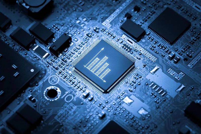
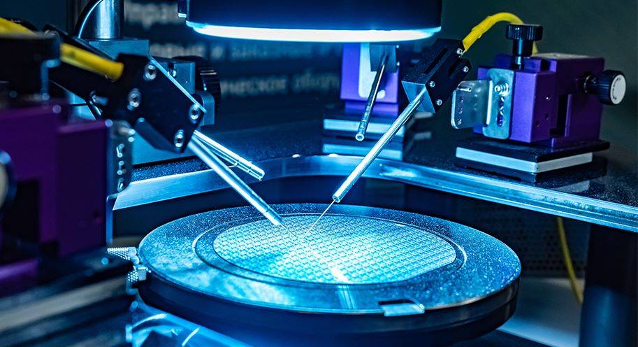
Semiconductor Manufacturing
PECVD (Plasma Enhanced Chemical Vapor Deposition) is a cornerstone in the semiconductor industry, playing a pivotal role in the fabrication of various critical components. This technique is primarily employed for the deposition of gate dielectrics, passivation layers, and interconnects, which are essential for the functionality and reliability of semiconductor devices.
Key Roles of PECVD in Semiconductor Manufacturing
| Component | Role |
|---|---|
| Gate Dielectrics | Acts as a barrier between the gate electrode and the semiconductor body, controlling the flow of current and preventing leakage. |
| Passivation Layers | Protects the device from environmental damage, enhancing durability and performance. |
| Interconnects | Facilitates the connection between different parts of the semiconductor, ensuring efficient signal transmission. |
PECVD's ability to deposit high-quality films at lower temperatures compared to traditional CVD methods makes it particularly suitable for semiconductor manufacturing. This low-temperature processing capability is crucial as it prevents damage to delicate device structures that are susceptible to high-temperature effects.
Moreover, PECVD's excellent film uniformity ensures that the deposited layers are of consistent thickness and composition across the substrate, which is vital for maintaining device performance and reliability. The high deposition rates offered by PECVD further contribute to its efficiency and cost-effectiveness in large-scale manufacturing processes.
In summary, PECVD's unique capabilities make it an indispensable tool in semiconductor manufacturing, enabling the creation of advanced devices with superior performance and reliability.
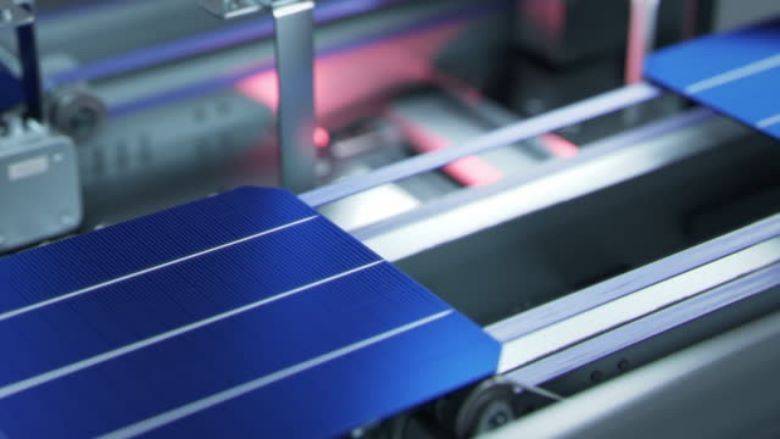
Solar Cell Manufacturing
PECVD (Plasma Enhanced Chemical Vapor Deposition) is a cornerstone in the manufacturing of solar cells and photovoltaic devices. Its unique capabilities are instrumental in creating thin, uniform films that are essential for the performance and efficiency of solar panels.
One of the key applications of PECVD in solar cell manufacturing is the deposition of anti-reflective coatings. These coatings are crucial for reducing the reflection of sunlight, thereby enhancing the absorption of light by the solar cells. By minimizing light reflection, PECVD-deposited anti-reflective coatings significantly improve the energy conversion efficiency of solar panels.
In addition to anti-reflective coatings, PECVD is also used to deposit other functional layers that contribute to the overall performance of solar cells. For instance, PECVD can be employed to create passivation layers that reduce surface recombination, thereby increasing the cell's efficiency. These layers are typically made from materials such as silicon nitride (SiN) and silicon dioxide (SiO₂), which offer excellent dielectric properties and thermal stability.
The versatility of PECVD in handling a wide range of materials, including amorphous silicon (a-Si) and diamond-like carbon (DLC), further extends its utility in solar cell manufacturing. These materials can be tailored to meet specific requirements, such as enhancing durability or improving electrical conductivity, making PECVD an indispensable tool in the production of high-performance solar cells.
Optical Coatings
PECVD (Plasma Enhanced Chemical Vapor Deposition) technology is instrumental in producing a wide array of optical coatings, ranging from those used in everyday items like sunglasses to sophisticated devices such as photometers and optical data storage systems. By meticulously managing plasma parameters, including pressure, temperature, and gas flow rates, the refractive index and other critical optical properties of the deposited films can be precisely adjusted. This fine-tuning allows for the creation of coatings that meet specific optical requirements, enhancing the performance of various optical devices.
In the realm of optical coatings, PECVD offers several advantages. For instance, it can produce anti-reflection coatings that minimize light loss in solar panels, thereby improving energy conversion efficiency. Similarly, high reflective coatings for laser optics are achieved through the deposition of thin films, ensuring optimal performance in laser applications. Additionally, PECVD is utilized to create infrared reflecting coatings, which increase the luminous flux intensity in filament lamps, making them more energy-efficient.
One of the standout features of PECVD is its ability to deposit thin films on optical fibers, enhancing their refractive and absorption coefficient performance. This is particularly crucial in telecommunications, where optical fibers need to transmit data over long distances with minimal loss. Furthermore, PECVD is employed in the production of protective coatings for optical data storage devices, safeguarding them from temperature fluctuations and other environmental factors that could compromise their integrity.
Biomedical Devices
PECVD technology has emerged as a pivotal tool in the manufacturing of biomedical devices, particularly medical implants. The process excels in depositing biocompatible, high-purity coatings that can be tailored to meet specific functional requirements. This capability is crucial for enhancing the performance and longevity of medical implants, which must interact safely with living tissues over extended periods.
One of the key advantages of PECVD in this context is its ability to operate at relatively low temperatures. This low-temperature processing is essential for preserving the structural integrity of the underlying materials, which is particularly important for delicate biomedical components. Additionally, PECVD allows for the deposition of a wide range of materials, including Silicon Nitride (SiN), Silicon Dioxide (SiO2), and Diamond-Like Carbon (DLC), each offering unique properties that can be harnessed to enhance the functionality of biomedical devices.
For instance, Silicon Nitride coatings can provide excellent dielectric properties and high thermal stability, making them ideal for insulating and protecting sensitive components. Silicon Dioxide, on the other hand, offers transparent dielectric properties that are valuable for optical and protective applications. Diamond-Like Carbon coatings, known for their high hardness and low friction, are particularly suited for applications requiring wear resistance, such as orthopedic implants.
Furthermore, the precision and control offered by PECVD enable the customization of coatings to meet specific biocompatibility and functionality requirements. This level of customization is critical for ensuring that the coatings not only protect the underlying material but also integrate seamlessly with the surrounding biological environment. As a result, PECVD has become an indispensable tool in the development of advanced biomedical devices, offering a versatile and reliable method for creating high-performance, biocompatible coatings.
Protective Coatings
PECVD technology is instrumental in creating dense nano-film protective coatings that offer a comprehensive shield for various materials. These coatings are characterized by their exceptional hydrophobicity, waterproofing, dustproofing, antimicrobial properties, and resistance to salt spray, corrosion, oxidation, and aging.
The multifunctional nature of these coatings makes them indispensable in several industries. For instance, in semiconductor manufacturing, these coatings provide vital protection to delicate electronic components, ensuring their longevity and reliability. Similarly, in solar cell manufacturing, the protective layers enhance the durability and efficiency of photovoltaic devices, making them more resilient to environmental factors.
Moreover, in biomedical applications, PECVD coatings are used to create biocompatible surfaces for implants and medical devices, reducing the risk of infection and improving the overall functionality of these devices. The ability to tailor these coatings to specific requirements further extends their utility, making them a versatile solution for a wide array of protective needs.
Future Trends of PECVD
Emerging Applications
In the future, PECVD is poised to maintain its pivotal role within the electronics industry, driven by a plethora of emerging applications and technological advancements. Key areas of growth include the development of novel materials, the seamless integration with other deposition technologies, and continuous R&D efforts aimed at enhancing the efficiency and versatility of PECVD systems.
Novel Materials
The exploration of new materials is a significant driver of PECVD's evolution. Researchers are delving into the potential of materials such as graphene, transition metal dichalcogenides, and perovskites, which offer unique properties that could revolutionize the functionality and performance of electronic devices. For instance, graphene's exceptional electrical conductivity and mechanical strength make it a promising candidate for next-generation transistors and flexible electronics.
Integration with Other Technologies
The integration of PECVD with other deposition techniques, such as Atomic Layer Deposition (ALD) and Physical Vapor Deposition (PVD), is another exciting frontier. This hybrid approach allows for the creation of multi-layered structures with tailored properties, enabling the fabrication of more complex and high-performance devices. For example, combining PECVD with ALD can produce ultra-thin, high-k dielectric layers that are crucial for advanced semiconductor devices.
Ongoing R&D Efforts
Research and development efforts are continually pushing the boundaries of what PECVD can achieve. Innovations in plasma generation methods, process parameter optimization, and in-situ monitoring techniques are leading to more efficient and precise deposition processes. These advancements not only improve the quality and uniformity of deposited films but also expand the range of applications for PECVD, from microelectronics to renewable energy and beyond.
Table: Emerging Applications of PECVD
| Application Area | Key Developments |
|---|---|
| Novel Materials | Exploration of graphene, transition metal dichalcogenides, and perovskites. |
| Integration | Seamless integration with ALD and PVD for multi-layered structures. |
| R&D Efforts | Innovations in plasma generation, process optimization, and in-situ monitoring. |
As these emerging applications take shape, PECVD's role in the electronics industry is set to become even more integral, driving the next wave of technological advancements and market growth.
Market Growth
The PECVD market is poised for substantial growth in the foreseeable future. Several key factors are driving this expansion, each contributing to the increasing adoption and integration of PECVD technology across various industries.
Firstly, the escalating demand for advanced electronic devices is a primary catalyst. As consumer electronics continue to evolve, the need for more sophisticated and efficient semiconductor components grows. PECVD's ability to deposit high-quality films at lower temperatures makes it an indispensable tool in semiconductor manufacturing, ensuring the production of reliable and high-performance devices.
Secondly, the development of new materials and processes is another significant driver. PECVD's versatility allows for the deposition of a wide range of materials, including silicon nitride, silicon dioxide, amorphous silicon, and diamond-like carbon, each with unique properties suited for specific applications. The ongoing research and development in this field are not only expanding the material options but also enhancing the quality and efficiency of the deposition process.
Lastly, the integration of PECVD with other deposition technologies is further fueling market growth. By combining PECVD with other techniques, manufacturers can leverage complementary strengths, optimizing the overall process and expanding the range of applications. This integration is particularly beneficial in industries such as semiconductor manufacturing, solar cell production, and optical coatings, where precision and efficiency are paramount.
Related Products
- Inclined Rotary Plasma Enhanced Chemical Vapor Deposition PECVD Equipment Tube Furnace Machine
- Chemical Vapor Deposition CVD Equipment System Chamber Slide PECVD Tube Furnace with Liquid Gasifier PECVD Machine
- Inclined Rotary Plasma Enhanced Chemical Vapor Deposition PECVD Equipment Tube Furnace Machine
- RF PECVD System Radio Frequency Plasma-Enhanced Chemical Vapor Deposition RF PECVD
- Multi Heating Zones CVD Tube Furnace Machine Chemical Vapor Deposition Chamber System Equipment
Related Articles
- Applications of PECVD Nano-Coating Technology in Electronic Devices
- A Comprehensive Guide to PECVD Equipment Maintenance
- PECVD Furnace A Low-Power and Low-Temperature Solution for Soft Matter
- Comparing the Performance of PECVD and HPCVD in Coating Applications
- Core Barriers to PECVD Nano-Coating Technology


