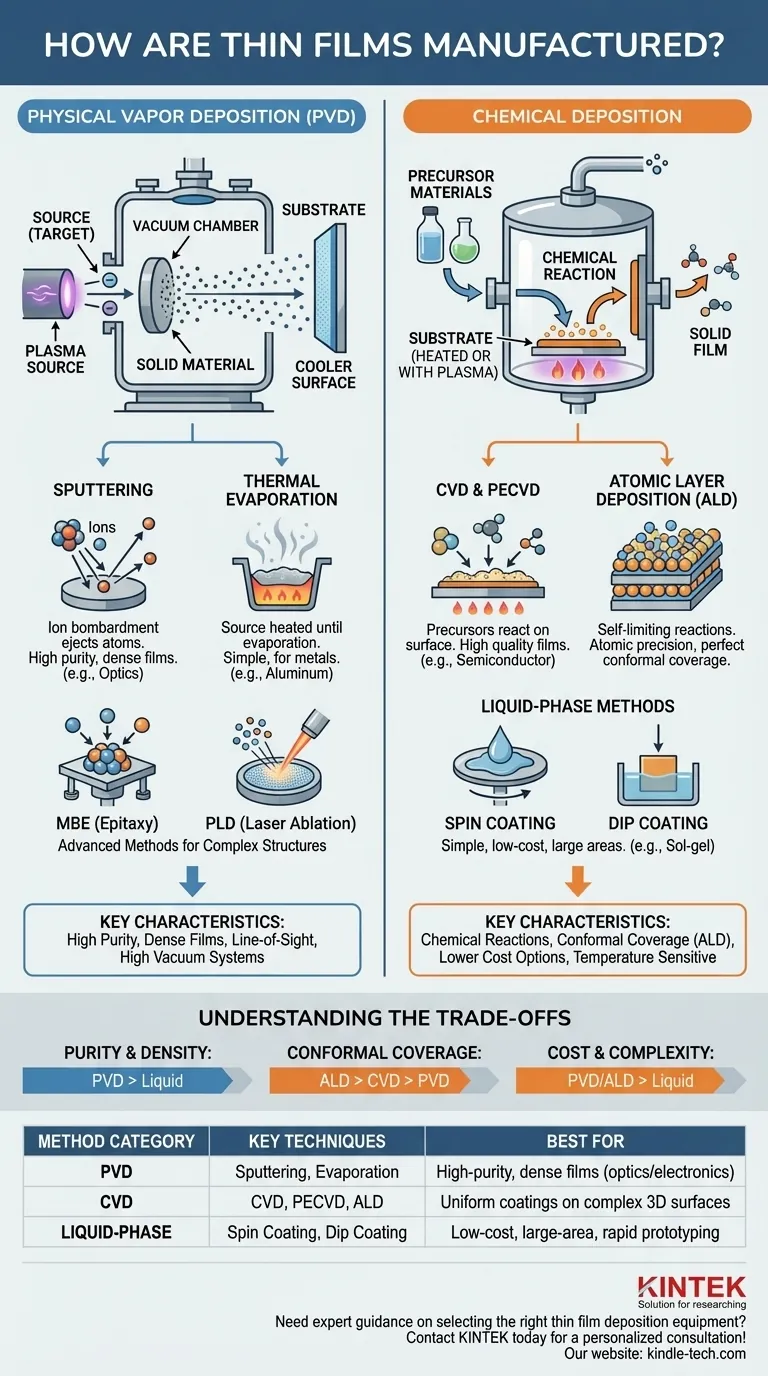
At its core, thin film manufacturing is a process known as deposition. All techniques for creating thin films, which are layers of material ranging from a few nanometers to several micrometers in thickness, fall into two primary categories: Physical Deposition and Chemical Deposition. These methods provide precise control over the thickness, composition, and properties of the final film.
The critical distinction is how the material arrives at the surface. Physical methods transport an existing solid material onto the substrate, while chemical methods use chemical reactions to create a new solid material directly on the substrate's surface. Your choice between them depends entirely on the film properties you need to achieve.
The Two Pillars of Deposition: Physical vs. Chemical
Understanding the fundamental difference between physical and chemical deposition is the key to navigating the landscape of thin film manufacturing. Each approach has a distinct philosophy and application.
What is Physical Vapor Deposition (PVD)?
Physical Vapor Deposition encompasses a family of methods that transfer material from a solid source (called a "target") to the substrate without changing its chemical composition.
The process involves energizing the source material in a vacuum chamber, causing it to vaporize. This vapor then travels and condenses onto the cooler substrate, forming a thin, solid film.
Think of it as moving material from one place to another on an atomic scale.
What is Chemical Deposition?
Chemical deposition methods use chemical reactions to form the film. Precursor materials, often in liquid or gas form, are introduced to the substrate.
A chemical reaction, frequently triggered by heat or plasma, occurs at the substrate's surface. This reaction produces the desired solid material as a byproduct, which then grows into a film.
This is a process of creation, where you build the film from chemical building blocks.
A Closer Look at Physical Deposition Methods
PVD methods are workhorses in industries like optics and microelectronics, prized for producing dense and pure films.
Sputtering
In sputtering, a target of the desired film material is bombarded with high-energy ions, typically from a gas like argon. This is like an atomic-scale game of billiards.
The ion collision ejects, or "sputters," atoms from the target. These ejected atoms then travel and coat the substrate, forming a very dense and uniform film.
Thermal Evaporation
Thermal evaporation is conceptually simpler. A source material is heated in a high vacuum until it evaporates into a gas.
This gas then expands within the chamber, eventually condensing on the relatively cool substrate to form a film. This method is common for depositing metals like aluminum or gold.
Advanced PVD: MBE and PLD
For cutting-edge research and highly complex electronics, more advanced PVD methods exist.
Molecular Beam Epitaxy (MBE) offers exquisite, single-crystal layer growth, while Pulsed Laser Deposition (PLD) uses a high-power laser to ablate material from a target, creating a plasma plume that deposits as a film.
Exploring Chemical Deposition Methods
Chemical methods offer unique advantages, especially in coating complex shapes and achieving atomic-level precision.
Chemical Vapor Deposition (CVD)
In CVD, precursor gases are introduced into a reaction chamber containing the substrate. Heat causes these gases to react and decompose on the substrate's surface, leaving behind a high-quality solid film.
A common variant is Plasma-Enhanced CVD (PECVD), which uses a plasma to enable these reactions at lower temperatures, protecting sensitive substrates.
Atomic Layer Deposition (ALD)
ALD is the gold standard for precision. It builds the film one single atomic layer at a time through a sequence of self-limiting chemical reactions.
This process provides unparalleled control over thickness and allows for perfectly uniform coatings on extremely complex, three-dimensional structures.
Liquid-Phase Methods: Spin Coating and Dip Coating
Not all chemical methods require complex vacuum systems. Spin coating involves dispensing a liquid precursor onto a substrate and spinning it at high speed to produce a thin, uniform layer as the solvent evaporates.
Sol-gel and dip coating are other liquid-based methods where a substrate is withdrawn from a chemical bath, leaving behind a film that is then cured with heat. These methods are often lower in cost and ideal for large-area applications.
Understanding the Trade-offs
No single method is universally best. The optimal choice is a function of specific engineering and economic requirements.
Purity and Density
PVD methods, especially sputtering, generally produce films with higher purity and density compared to most liquid-phase chemical methods. This is critical for high-performance optical and electronic applications.
Conformal Coverage
This is a major differentiator. Line-of-sight PVD methods struggle to uniformly coat complex shapes with high aspect ratios. Chemical methods like CVD and especially ALD excel at this, producing a perfectly conformal film over any surface topography.
Cost and Complexity
High-vacuum PVD and ALD systems represent a significant capital investment. In contrast, liquid-phase methods like spin coating, dip coating, or spray pyrolysis can be dramatically cheaper and simpler to implement.
Temperature Sensitivity
Many CVD processes require high temperatures that can damage certain substrates, such as polymers. PVD or lower-temperature PECVD can be a better choice in these cases.
Making the Right Choice for Your Application
Selecting a manufacturing method requires aligning the process capabilities with your end goal.
- If your primary focus is high-purity, dense films for optics or electronics: PVD methods like sputtering or evaporation are your starting point due to their excellent film quality.
- If you need to uniformly coat complex, non-flat surfaces: Chemical methods like CVD or the highly precise ALD are superior for their exceptional conformal coverage.
- If your goal is rapid prototyping or low-cost, large-area coating: Simple liquid-phase methods like spin coating or spray pyrolysis are often the most practical and economical choice.
Understanding these fundamental principles empowers you to select the deposition technique that aligns perfectly with your material, budget, and performance goals.
Summary Table:
| Method Category | Key Techniques | Best For |
|---|---|---|
| Physical Vapor Deposition (PVD) | Sputtering, Thermal Evaporation | High-purity, dense films for optics/electronics |
| Chemical Vapor Deposition (CVD) | CVD, PECVD, ALD | Uniform coatings on complex 3D surfaces |
| Liquid-Phase Methods | Spin Coating, Dip Coating | Low-cost, large-area coatings & rapid prototyping |
Need expert guidance on selecting the right thin film deposition equipment for your lab?
KINTEK specializes in lab equipment and consumables, serving laboratory needs. Our experts can help you choose the ideal PVD, CVD, or coating system to achieve precise film properties, improve your process efficiency, and stay within budget.
Contact our team today for a personalized consultation!
Visual Guide