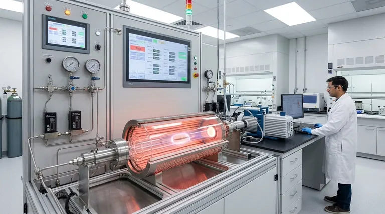
In essence, a Chemical Vapor Deposition (CVD) machine works by building a solid, high-performance material directly onto a surface from a gas. It introduces one or more volatile chemical gases, known as precursors, into a reaction chamber containing the object to be coated (the substrate). Energy, typically in the form of heat, is applied to the substrate, triggering a chemical reaction that causes the precursors to decompose and deposit a thin, solid film onto the surface, atom by atom.
The crucial concept to grasp is that CVD is not simply a coating method; it's a bottom-up manufacturing process. Instead of applying a pre-made substance, it synthesizes a new, solid material directly on a target surface through controlled chemical reactions, offering unparalleled purity and precision.
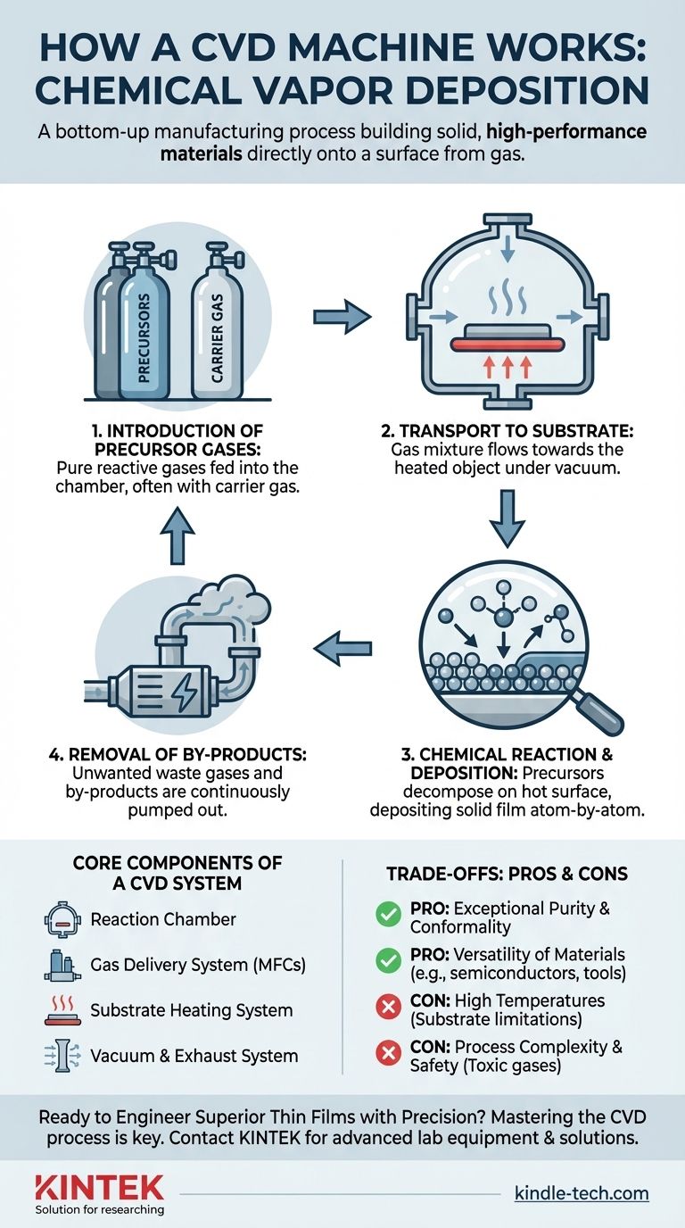
The Fundamental Stages of a CVD Process
To understand how a CVD machine operates, it's best to break the process down into a sequence of core physical and chemical events. Each stage must be precisely controlled to achieve the desired material properties.
Step 1: Introduction of Precursor Gases
The process begins by feeding highly pure, reactive gases called precursors into a sealed reaction chamber. These precursors contain the specific atoms needed for the final film (e.g., silicon, carbon, nitrogen).
Often, an inert carrier gas like argon or nitrogen is used to dilute the precursors and transport them through the system at a controlled rate.
Step 2: Transport to the Substrate
Inside the chamber, which is typically under a vacuum or controlled low pressure, the precursor gas mixture flows towards the substrate.
This transport is governed by principles of gas dynamics, including diffusion and convection, ensuring the reactant molecules reach the entire surface area of the object being coated.
Step 3: The Chemical Reaction and Deposition
This is the heart of the CVD process. The substrate is heated to a precise temperature, providing the thermal energy needed to initiate a chemical reaction.
When the precursor molecules come into contact with the hot surface, they adsorb (stick to the surface) and decompose. This chemical reaction breaks the molecules apart, leaving the desired solid atoms to bond with the substrate surface.
This deposition builds up the thin film, one atomic layer at a time, resulting in a dense, pure, and highly adherent material.
Step 4: Removal of By-products
The chemical reactions that form the solid film also create unwanted gaseous by-products.
These waste gases are continuously removed from the reaction chamber by the gas flow and vacuum system. This is critical for preventing contamination and ensuring the growing film remains pure.
Core Components of a CVD System
A functional CVD machine is an integration of several sophisticated subsystems, each playing a vital role in controlling the deposition process.
The Reaction Chamber
This is the sealed enclosure, often made of quartz or stainless steel, where the deposition takes place. It's designed to withstand high temperatures and maintain a controlled, ultra-clean vacuum environment.
The Gas Delivery System
This system precisely meters and mixes the precursor and carrier gases. It uses components like Mass Flow Controllers (MFCs) to ensure the exact chemical recipe is delivered to the chamber consistently.
The Substrate Heating System
Energy is required to drive the reaction. In most common CVD systems, this is a heating element (like a resistive heater or induction coil) that brings the substrate holder, and thus the substrate itself, to the target temperature.
The Vacuum and Exhaust System
This system, consisting of pumps and pressure gauges, serves two purposes. It first removes air and impurities to create a clean environment, and then it maintains the low pressure needed for the process while actively removing the gaseous by-products.
Understanding the Trade-offs
Like any advanced manufacturing process, CVD has distinct advantages and limitations that make it suitable for specific applications.
Pro: Exceptional Purity and Conformality
Because the material is built atom-by-atom from a pure gas source, CVD films have exceptionally high purity. The process is also highly conformal, meaning it can uniformly coat complex, three-dimensional shapes.
Pro: Versatility of Materials
CVD is an extremely versatile technology used to create a wide range of inorganic materials, including high-purity silicon for microchips, super-hard carbides and nitrides for cutting tools, and transparent oxides for optics.
Con: High Temperatures and Substrate Limitations
Traditional thermal CVD requires very high temperatures (often >600°C), which can damage or warp temperature-sensitive substrates like plastics or certain metals. This has led to the development of lower-temperature variants like Plasma-Enhanced CVD (PECVD).
Con: Process Complexity and Safety
The chemistry involved in CVD can be complex and difficult to control. Furthermore, many precursor gases are highly toxic, flammable, or corrosive, requiring stringent safety protocols and handling procedures.
How to Apply This to Your Goal
Your specific objective determines which aspect of the CVD process is most critical to your success.
- If your primary focus is semiconductor manufacturing: You must prioritize the extreme purity of precursor gases and the atomic-level precision of the deposition rate to build flawless crystalline layers.
- If your primary focus is creating wear-resistant coatings for tools: Your main concern will be achieving excellent adhesion and creating a dense, hard material like titanium nitride, which requires precise control over temperature and gas chemistry.
- If your primary focus is coating heat-sensitive materials: You must move beyond traditional thermal CVD and explore low-temperature alternatives like PECVD, where plasma provides the reaction energy instead of just heat.
Ultimately, mastering the CVD process is about controlling a chemical reaction on a surface to engineer materials with precisely the properties you need.
Summary Table:
| Stage | Key Action | Purpose |
|---|---|---|
| 1. Gas Introduction | Precursor gases are fed into the chamber. | Deliver the atomic building blocks for the film. |
| 2. Gas Transport | Gases flow and diffuse towards the heated substrate. | Ensure uniform coverage of the target surface. |
| 3. Reaction & Deposition | Precursors decompose on the hot surface, depositing a solid film. | Build the material atom-by-atom for high purity and adhesion. |
| 4. By-product Removal | Waste gases are pumped out of the chamber. | Maintain a clean environment and prevent contamination. |
Ready to Engineer Superior Thin Films with Precision?
Whether you are developing next-generation semiconductors, creating ultra-hard wear-resistant coatings, or need to coat complex 3D shapes, mastering the CVD process is key to your success. KINTEK specializes in providing the advanced lab equipment and consumables you need to achieve unparalleled purity, conformity, and material performance.
Let's discuss how our expertise can help you:
- Select the right CVD technology for your specific substrate and material goals.
- Optimize your process parameters for maximum efficiency and yield.
- Ensure safe handling of precursor gases and by-products.
Contact our experts today to explore the perfect CVD solution for your laboratory's unique challenges.
Visual Guide
Related Products
- HFCVD Machine System Equipment for Drawing Die Nano-Diamond Coating
- Microwave Plasma Chemical Vapor Deposition MPCVD Machine System Reactor for Lab and Diamond Growth
- Multi Heating Zones CVD Tube Furnace Machine Chemical Vapor Deposition Chamber System Equipment
- Chemical Vapor Deposition CVD Equipment System Chamber Slide PECVD Tube Furnace with Liquid Gasifier PECVD Machine
- CVD Diamond Dressing Tools for Precision Applications
People Also Ask
- What is the function of tungsten filaments in HFCVD? Powering Diamond Film Synthesis with Thermal Excitation
- What is the chemical vapor deposition growth process? Build Superior Thin Films from the Atom Up
- What are the advantages of chemical vapor deposition? Achieve Superior Thin Films for Your Lab
- What types of substrates are used in CVD to facilitate graphene films? Optimize Graphene Growth with the Right Catalyst
- How expensive is chemical vapor deposition? Understanding the True Cost of High-Performance Coating