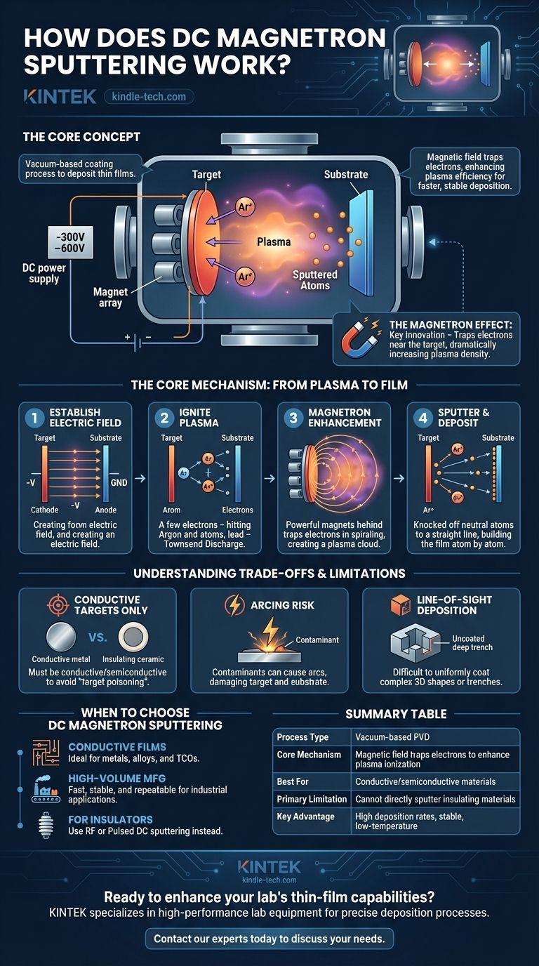
At its core, DC magnetron sputtering is a vacuum-based coating process used to deposit extremely thin films of material onto a surface. It functions by creating an energized gas plasma, which bombards a source material (the "target") with ions, knocking atoms loose. A precisely configured magnetic field enhances this process, guiding the dislodged atoms to coat a component (the "substrate") with a uniform, high-quality film.
The critical innovation of DC magnetron sputtering is not just the sputtering itself, but the use of a magnetic field. This field traps electrons near the target, dramatically increasing the efficiency of the plasma, which results in faster, more stable, and lower-temperature deposition compared to methods without a magnetron.
The Core Mechanism: From Plasma to Film
To understand how this process achieves such precise results, we must break it down into a sequence of physical events occurring within the vacuum chamber.
Establishing the Electric Field
First, the substrate to be coated and the target material are placed in a vacuum chamber, which is then pumped down to a low pressure and backfilled with an inert gas, typically Argon.
A strong DC voltage, often around -300V to -600V, is applied to the target, making it a cathode. The substrate holder is typically grounded, acting as the anode. This creates a powerful electric field between the two.
Igniting the Plasma
This electric field accelerates the few free electrons naturally present in the gas. As these high-speed electrons collide with neutral Argon atoms, they knock other electrons loose.
This event leaves behind positively charged Argon ions (Ar+) and creates more free electrons, which in turn ionize more atoms. This cascade effect, known as a Townsend discharge, rapidly forms a self-sustaining, glowing plasma.
The Role of the Magnetron
This is the key to the process's efficiency. A set of powerful permanent magnets is placed behind the target. This creates a magnetic field that projects out in front of the target's surface.
This magnetic field is too weak to affect the heavy Argon ions, but it is strong enough to trap the much lighter secondary electrons that are also ejected from the target during bombardment. These electrons are forced into a tight, spiraling path, creating a dense electron cloud directly in front of the target.
Enhancing Ionization Efficiency
Because these electrons are trapped in a long, looping path instead of traveling directly to the anode, their chances of colliding with and ionizing a neutral Argon atom increase dramatically.
This magnetic confinement creates a far denser and more intense plasma than would be possible with just the electric field. This is the "magnetron" effect, and it is what makes the sputtering process so fast and stable.
Sputtering the Target
The positively charged Argon ions in the dense plasma are not trapped by the magnetic field. Instead, they are aggressively accelerated by the negative voltage of the target.
They strike the target surface with immense kinetic energy. If the energy transferred in a collision is greater than the material's atomic binding energy, it knocks loose, or "sputters," a neutral atom from the target material.
Deposition on the Substrate
These sputtered, neutral atoms are unaffected by the electric or magnetic fields. They travel in straight lines through the vacuum until they strike a surface.
As they land on the substrate, they condense and slowly build up, atom by atom, to form a dense, uniform, and very thin film of the target material.
Understanding the Trade-offs and Limitations
While powerful, DC magnetron sputtering is not a universal solution. Its effectiveness is defined by specific physical constraints.
The Target Material Constraint
The primary limitation of the DC method is that the target material must be electrically conductive or at least semiconductive.
If the target were an insulator (like a ceramic), the constant bombardment by positive Argon ions would cause a positive charge to build up on its surface. This effect, known as "target poisoning," would neutralize the negative bias, repel incoming ions, and quickly extinguish the sputtering process.
The Problem of Arcing
Even with conductive targets, small insulating contaminants or oxides on the surface can accumulate charge. This can lead to a sudden, high-current discharge known as an arc, which can damage the target and the substrate, and disrupt the film's uniformity. This is why a related technique, Pulsed DC sputtering, was developed to coat insulating materials by periodically reversing the voltage to discharge the target.
Line-of-Sight Deposition
Since the sputtered atoms are neutral, they travel in a straight line from the target to the substrate. This makes it difficult to uniformly coat complex, three-dimensional shapes with sharp edges or deep trenches. Achieving good "step coverage" often requires sophisticated substrate rotation and manipulation during deposition.
When to Choose DC Magnetron Sputtering
Understanding these principles allows you to select the right process for your specific goal.
- If your primary focus is depositing conductive films: DC magnetron sputtering is the ideal, most cost-effective, and efficient method for depositing metals, alloys, and transparent conductive oxides (TCOs).
- If your primary focus is depositing insulating films: Standard DC sputtering is unsuitable; you must consider alternatives like RF (Radio Frequency) sputtering or Pulsed DC sputtering, which are designed to handle non-conductive materials.
- If your primary focus is high-volume manufacturing: The speed, stability, and precise repeatability of DC magnetron sputtering make it a foundational technology for industrial applications, from semiconductor fabrication to coating architectural glass.
By mastering the interplay of electric and magnetic fields, DC magnetron sputtering provides engineers and scientists with a precise and powerful tool for engineering materials at the atomic scale.
Summary Table:
| Key Aspect | Description |
|---|---|
| Process Type | Vacuum-based Physical Vapor Deposition (PVD) |
| Core Mechanism | Magnetic field traps electrons to enhance plasma ionization |
| Best For | Conductive/semiconductive materials (metals, alloys, TCOs) |
| Primary Limitation | Cannot directly sputter insulating materials |
| Key Advantage | High deposition rates, stable process, low-temperature operation |
Ready to enhance your lab's thin-film capabilities? KINTEK specializes in high-performance lab equipment and consumables for precise deposition processes like DC magnetron sputtering. Whether you're in semiconductor research, materials science, or industrial coating, our solutions deliver the uniformity and reliability your work demands. Contact our experts today to discuss how we can support your laboratory's specific needs with tailored equipment and consumables.
Visual Guide
Related Products
- Chemical Vapor Deposition CVD Equipment System Chamber Slide PECVD Tube Furnace with Liquid Gasifier PECVD Machine
- Microwave Plasma Chemical Vapor Deposition MPCVD Machine System Reactor for Lab and Diamond Growth
- HFCVD Machine System Equipment for Drawing Die Nano-Diamond Coating
- Customer Made Versatile CVD Tube Furnace Chemical Vapor Deposition Chamber System Equipment
- 915MHz MPCVD Diamond Machine Microwave Plasma Chemical Vapor Deposition System Reactor
People Also Ask
- How are carbon nanotubes grown? Master Scalable Production with Chemical Vapor Deposition
- What happens during deposition chemistry? Building Thin Films from Gaseous Precursors
- Why is Chemical Vapor Deposition (CVD) equipment uniquely suited for constructing hierarchical superhydrophobic structures?
- What is plasma enhanced chemical vapor deposition PECVD equipment? A Guide to Low-Temperature Thin Film Deposition
- What are the core advantages of PE-CVD in OLED encapsulation? Protect Sensitive Layers with Low-Temp Film Deposition


