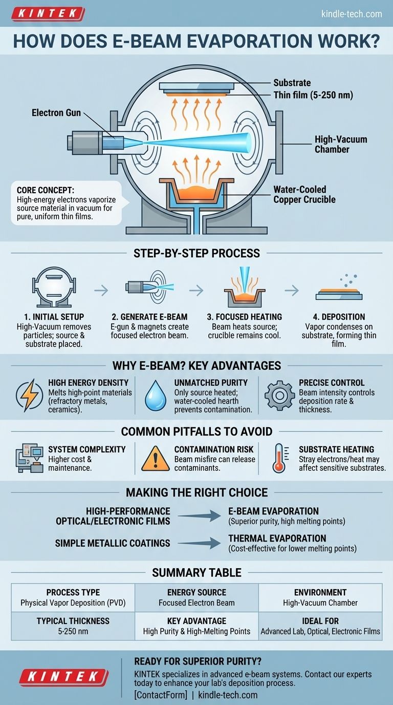
At its core, e-beam evaporation is a high-precision process that uses a focused beam of high-energy electrons to heat and vaporize a source material inside a vacuum chamber. This vapor then travels upward and condenses onto a cooler substrate, forming an exceptionally pure and uniform thin film. The process allows for the deposition of materials with very high melting points, which is a significant advantage over other methods.
Electron-beam evaporation isn't just about heating a material; it's about delivering a massive amount of energy with surgical precision. This targeted approach allows it to vaporize otherwise difficult materials, resulting in thin films of superior purity and quality.
The E-Beam Evaporation Process, Step-by-Step
To understand how this technique achieves such high-quality results, it's best to break it down into its core stages. Each step is carefully controlled to ensure the final film meets exact specifications.
The Initial Setup
The entire process occurs within a high-vacuum chamber. This vacuum is critical because it removes atmospheric particles, allowing the evaporated material to travel directly to the substrate without collisions or contamination.
Inside the chamber, the source material (the material to be deposited) is placed in a water-cooled copper hearth or crucible. The substrate (the object to be coated) is positioned directly above this source.
Generating the Electron Beam
A specialized electron gun generates a beam of electrons and accelerates them to a high energy level. Magnetic fields are used to precisely focus and steer this beam, directing it to strike the surface of the source material in the crucible.
Focused Heating and Evaporation
When the high-energy electron beam hits the source material, it transfers its kinetic energy almost instantly, generating intense, localized heat. This allows the material's surface to reach its evaporation point very quickly.
Because the energy is delivered directly to the material, the surrounding crucible remains cool, a key feature made possible by the water-cooled hearth. The material turns into a vapor, which then rises from the source.
Deposition and Film Formation
The evaporated atoms or molecules travel in a straight line through the vacuum until they reach the cooler substrate. Upon contact, they condense and bond to the substrate's surface, gradually building a thin film.
This process creates films that are typically between 5 and 250 nanometers thick, altering the substrate's optical, electrical, or physical properties without changing its fundamental shape.
Why E-Beam? Key Advantages Over Traditional Methods
E-beam evaporation is a type of Physical Vapor Deposition (PVD), but it offers distinct advantages over the simpler method of thermal (or resistive) evaporation, where a material is heated by passing a current through its container.
High Energy Density
E-beam evaporation can deliver a far greater concentration of energy than thermal methods. This allows it to melt and vaporize materials with extremely high melting points, such as refractory metals and ceramics, that are impossible to deposit with a standard resistance boat.
Unmatched Film Purity
In thermal evaporation, the entire boat or coil holding the material is heated, which can cause the container itself to outgas or contaminate the film. With e-beam, only the source material is heated, while the water-cooled crucible stays cool. This dramatically reduces contamination and produces films of very high purity.
Precise Control Over Deposition Rate
The intensity of the electron beam can be controlled with high precision. This gives operators fine-grained control over the rate of evaporation, which in turn allows for precise management of the final film's thickness and uniformity.
Common Pitfalls to Avoid
While powerful, the e-beam process has complexities and trade-offs that are critical to understand for successful implementation.
System Complexity
E-beam systems are significantly more complex than their thermal counterparts. They require high-voltage power supplies, sophisticated magnetic steering systems, and more robust vacuum technology, leading to higher initial investment and maintenance costs.
Potential for Contamination
While the process produces high-purity films, improper beam control can be a source of problems. If the electron beam accidentally strikes the crucible wall or other components, it can release contaminants that degrade the quality of the film.
Substrate Heating
Although the energy is focused, some stray electrons and radiant heat can reach the substrate. For heat-sensitive substrates, this can be a significant issue, requiring careful process monitoring and potentially substrate cooling systems.
Making the Right Choice for Your Goal
Selecting the correct deposition method depends entirely on your material requirements and performance goals.
- If your primary focus is high-performance optical or electronic films: E-beam evaporation is the superior choice for depositing high-melting-point or dielectric materials where purity is paramount.
- If your primary focus is simple metallic coatings with less stringent purity needs: Traditional thermal evaporation is often a more direct and cost-effective solution for materials with lower melting points.
Ultimately, understanding this fundamental difference in energy delivery is the key to selecting the right tool for your specific material and performance requirements.
Summary Table:
| Key Aspect | E-Beam Evaporation Details |
|---|---|
| Process Type | Physical Vapor Deposition (PVD) |
| Energy Source | Focused beam of high-energy electrons |
| Environment | High-vacuum chamber |
| Typical Film Thickness | 5 to 250 nanometers |
| Key Advantage | Deposits high-melting-point materials with superior purity |
| Ideal For | High-performance optical coatings, electronic films |
Ready to achieve superior thin film purity for your lab?
E-beam evaporation is the gold standard for depositing high-melting-point materials like refractory metals and ceramics with exceptional purity and control. If your research or production demands high-performance optical or electronic films, the right equipment is critical.
KINTEK specializes in advanced lab equipment, including e-beam evaporation systems, to meet the precise needs of modern laboratories. Our expertise can help you select the perfect solution for your material and performance requirements.
Contact our experts today to discuss how our e-beam evaporation technology can enhance your deposition process and results.
Visual Guide
Related Products
- Electron Beam Evaporation Coating Oxygen-Free Copper Crucible and Evaporation Boat
- Electron Beam Evaporation Coating Tungsten Crucible and Molybdenum Crucible for High Temperature Applications
- Electron Beam Evaporation Coating Gold Plating Tungsten Molybdenum Crucible for Evaporation
- E Beam Crucibles Electron Gun Beam Crucible for Evaporation
- Electron Beam Evaporation Coating Conductive Boron Nitride Crucible BN Crucible
People Also Ask
- What is the deposition rate of e-beam evaporation? Control Thin Film Quality and Speed
- How is an electron beam evaporator cooled during deposition? Essential Thermal Management for Stable Processes
- What is the temperature of e-beam evaporation? Mastering the Two-Zone Thermal Process for Precision Films
- What are the applications of e-beam evaporation? Achieve High-Purity Coatings for Optics & Electronics
- What is the voltage of e-beam evaporation? Achieve Precise Thin-Film Deposition


