RF sputtering is a physical vapor deposition (PVD) technique that uses a radio frequency power source to create a plasma and deposit thin films of material onto a surface. Unlike its simpler counterpart, DC sputtering, this method is specifically designed to work with electrically insulating or dielectric materials, such as ceramics and oxides, by preventing a process-halting charge buildup on the target.
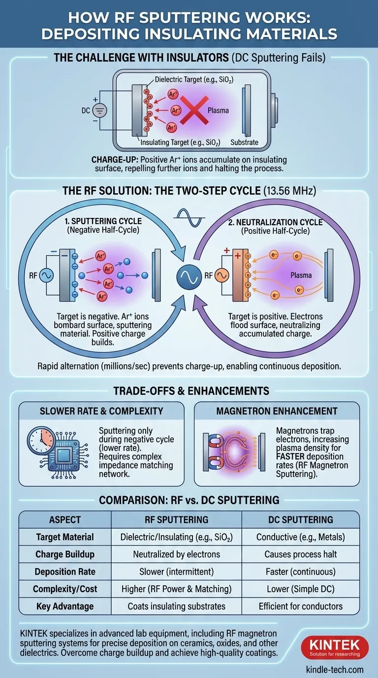
The core problem with depositing insulating materials is that they accumulate electrical charge, which repels the very ions needed for the sputtering process to continue. RF sputtering solves this by rapidly alternating the electric field, using one cycle to sputter the material and the subsequent cycle to attract electrons that neutralize the accumulated charge, enabling continuous deposition.
The Fundamental Sputtering Process
Sputtering, in any form, is a physical process, not a chemical one. Think of it as a microscopic game of atomic billiards.
Creating the Plasma Environment
The entire process takes place inside a high-vacuum chamber. This chamber is first evacuated and then backfilled with a small, controlled amount of an inert gas, almost always argon (Ar). This gas provides the "projectiles" for the process.
The Target and Substrate
Inside the chamber are two key components: the target and the substrate. The target is a plate made of the material you wish to deposit (e.g., silicon dioxide). The substrate is the object you want to coat (e.g., a silicon wafer). An electric field is established between them.
Ion Bombardment and Atom Ejection
When the electric field is applied, it energizes the argon gas, stripping electrons from the argon atoms and creating a glowing plasma composed of positive argon ions (Ar+) and free electrons. The positively charged argon ions are forcefully accelerated toward the negatively charged target.
Upon impact, these high-energy ions physically knock atoms loose from the target's surface. This ejection of target material is the "sputtering." These newly freed atoms then travel through the vacuum and land on the substrate, gradually building up a thin, uniform film.
Why Radio Frequency (RF) is the Critical Innovation
The basic process described above works perfectly well with a simple Direct Current (DC) power source if the target is electrically conductive, like a metal. However, if the target is an insulator, DC sputtering fails almost instantly.
The Challenge with Insulating Targets
With a DC power source, the target is held at a constant negative voltage. When positive Ar+ ions strike the insulating target, their charge has nowhere to go. They accumulate on the surface, creating a localized positive charge. This is known as "charge-up."
This positive charge buildup quickly becomes strong enough to repel any new Ar+ ions trying to approach, effectively shutting down the sputtering process.
The Two-Step RF Cycle
RF sputtering overcomes this by using an alternating current power source that oscillates at radio frequencies (typically 13.56 MHz). This rapid switching creates two distinct half-cycles.
- The Sputtering Cycle (Negative): During the half-cycle when the target is negatively charged, it attracts the positive Ar+ ions from the plasma. These ions bombard the surface and sputter material, just as in the DC process. However, this also causes positive charge to build up.
- The Neutralization Cycle (Positive): In the next half-cycle, the target's polarity flips to positive. It now strongly attracts the much lighter, more mobile free electrons from the plasma. These electrons flood the target's surface, neutralizing the positive charge accumulated during the previous cycle.
This rapid alternation, happening millions of times per second, allows for continuous sputtering of insulating materials without any process-halting charge-up.
Understanding the Trade-offs
While RF sputtering is exceptionally versatile, it's essential to understand its inherent compromises compared to other methods.
Slower Deposition Rates
Because effective sputtering only occurs during the negative portion of the RF cycle, the overall deposition rate is generally lower than that of DC sputtering for a given power level. The process is effectively "off" for half the time.
System Complexity and Cost
RF power systems are significantly more complex than DC power supplies. They require sophisticated impedance matching networks to efficiently transfer power to the plasma, which increases the cost and maintenance requirements of the equipment.
The Role of Magnetrons
To counteract the slower deposition rates, most modern systems use magnetron sputtering. By placing powerful magnets behind the target, the free electrons in the plasma are trapped in a magnetic field directly in front of the target's surface.
This electron trap dramatically increases the probability of collisions with argon gas atoms, creating a much denser, more ion-rich plasma right where it's needed. This allows for significantly faster deposition rates. When this is paired with an RF power source, it is called RF magnetron sputtering.
Making the Right Choice for Your Application
Selecting the correct sputtering technique depends entirely on the material you need to deposit and your performance requirements.
- If your primary focus is depositing conductive materials (e.g., metals like aluminum or titanium): DC magnetron sputtering is almost always the more efficient and cost-effective choice.
- If your primary focus is depositing non-conductive, dielectric materials (e.g., silicon dioxide, aluminum nitride): RF sputtering is the essential technology required to prevent target charge-up.
- If your primary focus is maximizing the deposition rate of an insulating material: RF magnetron sputtering provides the necessary charge neutralization of RF with the rate enhancement of magnetrons.
Ultimately, understanding the role of the alternating field is the key to leveraging RF sputtering for the advanced material layers that define modern technology.
Summary Table:
| Aspect | RF Sputtering | DC Sputtering |
|---|---|---|
| Target Material | Dielectric/Insulating (e.g., SiO₂, Al₂O₃) | Conductive (e.g., metals) |
| Charge Buildup | Neutralized by electron flooding | Causes process halt |
| Deposition Rate | Slower (sputters only during negative cycle) | Faster |
| Complexity/Cost | Higher (requires RF power & impedance matching) | Lower |
| Key Advantage | Enables coating of insulating substrates | Efficient for conductive materials |
Need to deposit thin films on challenging insulating materials? KINTEK specializes in advanced lab equipment, including RF magnetron sputtering systems designed for precise, uniform deposition on ceramics, oxides, and other dielectrics. Our solutions help you overcome charge buildup issues and achieve reliable, high-quality coatings for your research or production needs. Contact us today to discuss how our expertise can enhance your thin film processes!
Visual Guide
Related Products
- RF PECVD System Radio Frequency Plasma-Enhanced Chemical Vapor Deposition RF PECVD
- Spark Plasma Sintering Furnace SPS Furnace
- Horizontal High Temperature Graphite Vacuum Graphitization Furnace
People Also Ask
- How does plasma enhance CVD? Unlock Low-Temperature, High-Quality Film Deposition
- What is plasma chemical vapor deposition? A Low-Temperature Thin Film Coating Solution
- What is an example of PECVD? RF-PECVD for High-Quality Thin Film Deposition
- Why is a Matching Network Indispensable in RF-PECVD for Siloxane Films? Ensure Stable Plasma and Uniform Deposition
- What is the role of RF-PECVD in VFG preparation? Mastering Vertical Growth and Surface Functionality


