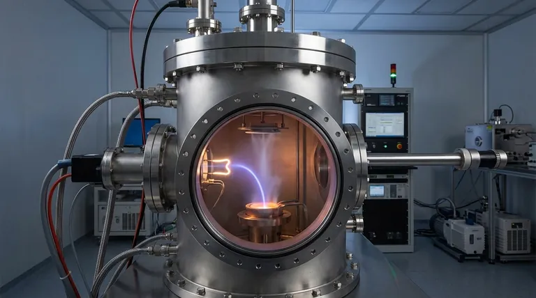
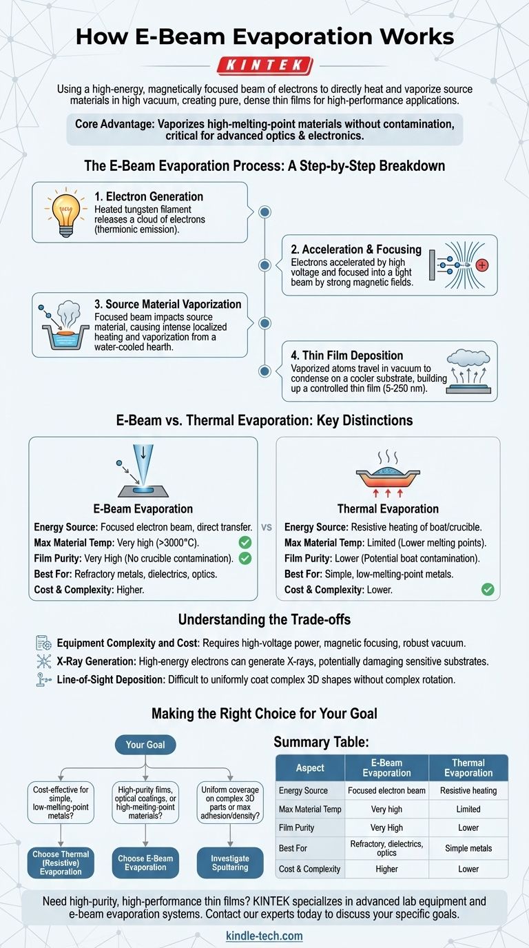
In essence, e-beam evaporation works by using a high-energy, magnetically focused beam of electrons to heat a source material in a high vacuum. This intense, localized heating causes the material to vaporize. The resulting vapor then travels upwards and condenses onto a cooler substrate, forming an extremely pure and dense thin film.
The core advantage of e-beam evaporation is its ability to directly heat and vaporize even very high-melting-point materials without contaminating the film, a significant limitation of simpler thermal methods. This makes it a critical process for high-performance optical and electronic applications.
The E-Beam Evaporation Process: A Step-by-Step Breakdown
To understand how this technique achieves such high-quality films, it is best to break the process down into its fundamental stages. Each step occurs within a high-vacuum chamber to ensure particle purity and a clear path for deposition.
Step 1: Electron Generation
The process begins at a heated filament, typically made of tungsten. A high current is passed through this filament, causing it to heat up and release a cloud of electrons through a process called thermionic emission.
Step 2: Acceleration and Focusing
These free electrons are then accelerated by a strong electric field, created by applying a high voltage (several kilovolts) between the filament (cathode) and the source material area (anode).
A powerful magnetic field is then used to precisely steer and focus these high-velocity electrons into a tight, concentrated beam.
Step 3: Source Material Vaporization
This high-energy electron beam is directed onto the source material, which is held in a water-cooled copper crucible or "hearth."
The kinetic energy of the electrons is converted into intense thermal energy upon impact, heating a small spot on the source material to its vaporization point. Because the crucible itself is water-cooled, only the target material evaporates, preventing contamination from the container.
Step 4: Thin Film Deposition
The vaporized atoms travel in a straight line from the source toward the substrate (the object to be coated), which is positioned above.
When the vaporized atoms reach the relatively cool surface of the substrate, they condense and bond to it, gradually building up a thin film. The thickness of this film, often between 5 and 250 nanometers, can be precisely controlled.
E-Beam vs. Thermal Evaporation: Key Distinctions
While both are forms of physical vapor deposition (PVD), e-beam evaporation addresses the core limitations of the simpler thermal (or resistive) evaporation method.
The Energy Source
In thermal evaporation, a boat or coil holding the source material is heated by passing an electric current through it. The material evaporates because it is in direct contact with this hot element.
In e-beam evaporation, energy is transferred directly to the source material via the electron beam, not through a secondary heating element. This allows for much higher energy density and more precise control.
Material Compatibility
Thermal evaporation is limited to materials with relatively low melting points. The heating boat itself can melt or react with the source material at higher temperatures.
E-beam evaporation excels at depositing refractory metals (like tungsten or tantalum) and dielectric compounds (like titanium dioxide or silicon dioxide) that have extremely high melting points.
Film Purity and Quality
Because thermal evaporation heats a boat or crucible, there is a risk that atoms from the boat itself will evaporate and become incorporated into the film as impurities.
E-beam evaporation produces significantly higher purity films because the water-cooled hearth remains cool, ensuring only the source material is vaporized. This leads to denser, higher-performance coatings.
Understanding the Trade-offs
Despite its advantages, e-beam evaporation is not the universal solution for all applications. Understanding its limitations is key to making an informed decision.
Equipment Complexity and Cost
E-beam systems are more complex and expensive than thermal evaporators. They require high-voltage power supplies, sophisticated magnetic focusing systems, and more robust vacuum chambers.
X-Ray Generation
The impact of high-energy electrons on the source material can generate X-rays. This radiation can potentially damage sensitive substrates, such as semiconductor devices or certain plastics, requiring careful process design or shielding.
Line-of-Sight Deposition
Like all evaporation techniques, e-beam is a "line-of-sight" process. The vapor travels in a straight line, which can make it difficult to uniformly coat complex, three-dimensional shapes without complex substrate rotation mechanisms.
Making the Right Choice for Your Goal
Selecting the correct deposition method depends entirely on your material requirements, budget, and desired film quality.
- If your primary focus is cost-effectiveness for simple, low-melting-point metals: Standard thermal (resistive) evaporation is often the most practical choice.
- If your primary focus is depositing high-purity films, optical coatings, or high-melting-point materials: E-beam evaporation is the superior and often necessary method.
- If your primary focus is achieving uniform coverage on complex 3D parts or maximizing film adhesion and density: You should investigate other PVD techniques, such as sputtering.
Ultimately, choosing the right deposition tool requires matching the technique's capabilities to the specific demands of your final product.
Summary Table:
| Aspect | E-Beam Evaporation | Thermal Evaporation |
|---|---|---|
| Energy Source | Focused electron beam | Resistive heating of a boat/crucible |
| Max Material Temp | Very high (>3000°C) | Limited (lower melting points) |
| Film Purity | Very High (no crucible contamination) | Lower (potential boat contamination) |
| Best For | Refractory metals, dielectrics, optics | Simple, low-melting-point metals |
| Cost & Complexity | Higher | Lower |
Need to deposit high-purity, high-performance thin films?
KINTEK specializes in advanced lab equipment, including e-beam evaporation systems designed for demanding applications in research and production. Our solutions help you achieve superior film quality for optics, semiconductors, and more.
Contact our experts today to discuss how our e-beam technology can meet your specific deposition goals.
Visual Guide
Related Products
- Electron Beam Evaporation Coating Oxygen-Free Copper Crucible and Evaporation Boat
- Electron Beam Evaporation Coating Tungsten Crucible and Molybdenum Crucible for High Temperature Applications
- Electron Beam Evaporation Coating Gold Plating Tungsten Molybdenum Crucible for Evaporation
- E Beam Crucibles Electron Gun Beam Crucible for Evaporation
- Electron Beam Evaporation Coating Conductive Boron Nitride Crucible BN Crucible
People Also Ask
- What are the applications of electron beams? From Nanoscale Imaging to Industrial Manufacturing
- What is e-beam evaporation used for? Precision Coating for Optics, Aerospace & Electronics
- What is e-beam evaporation? Achieve High-Purity Thin Film Deposition for Your Lab
- What is the temperature of e-beam evaporation? Mastering the Two-Zone Thermal Process for Precision Films
- What are the applications of e-beam evaporation? Achieve High-Purity Coatings for Optics & Electronics


