At its core, thin film deposition is a process of applying a microscopic layer of one material onto the surface of another. This technique involves transforming a source material into a vapor, transporting it through a controlled environment, and allowing it to condense onto a target object, known as a substrate. The resulting film, often just a few nanometers to micrometers thick, fundamentally changes the substrate's properties to improve its performance or grant it new capabilities.
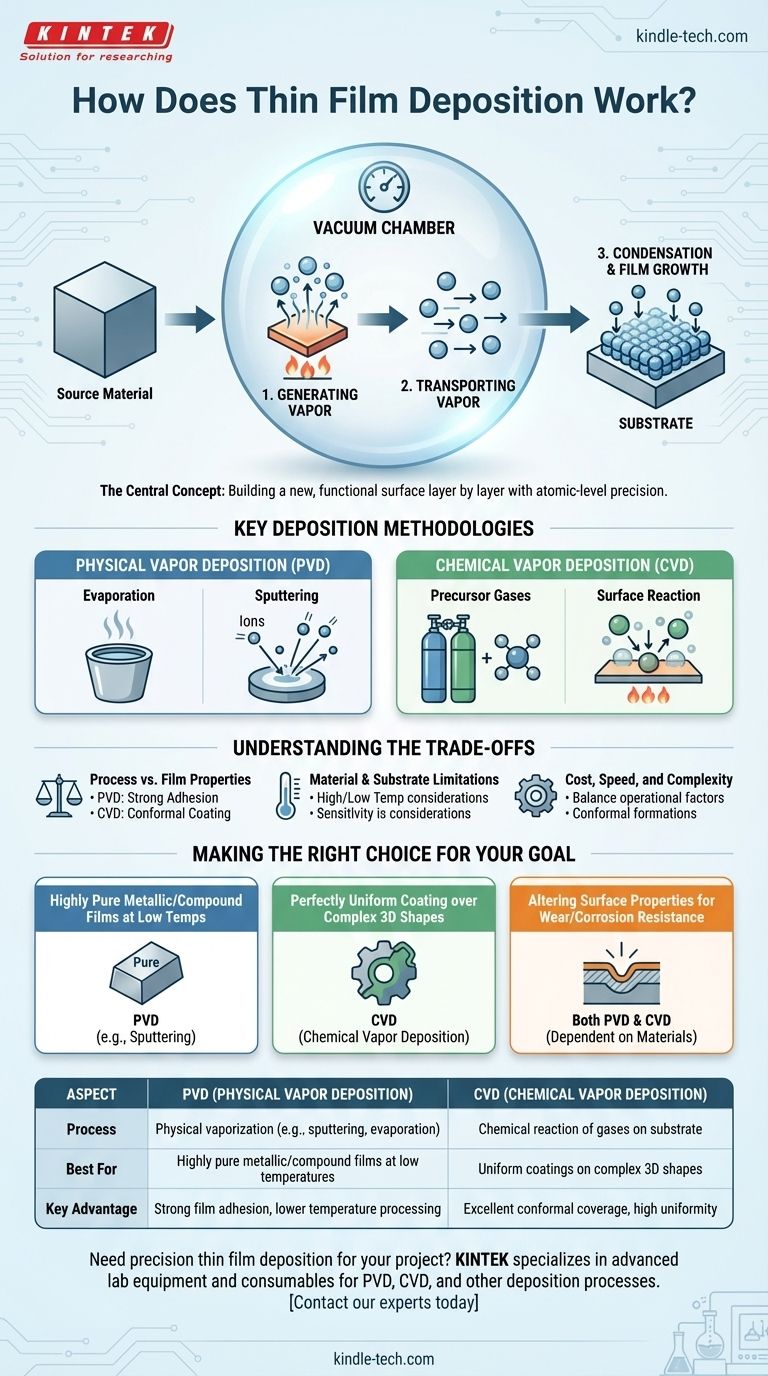
The central concept is not simply coating a surface, but building a new, functional surface layer by layer. All thin film deposition methods follow a fundamental sequence: creating a vapor from a source material, transporting it, and condensing it with atomic-level precision onto a substrate.
The Core Principle: From Source to Substrate
Nearly all deposition techniques can be understood as a three-step process. The specific method used for each step determines the characteristics of the final film and its suitability for a given application.
Step 1: Generating the Material Vapor
The first challenge is to convert the solid or liquid source material into a gas or vapor phase. This allows individual atoms or molecules to travel and deposit themselves onto the substrate. This is typically achieved through physical or chemical means.
Step 2: Transporting the Vapor
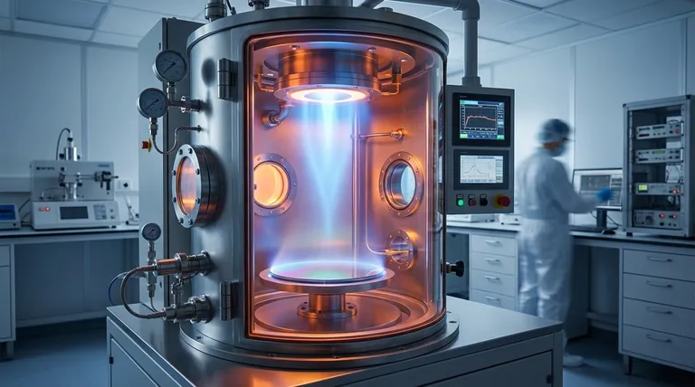
Once created, the vapor must travel from the source to the substrate. This almost always occurs within a vacuum chamber. The vacuum is critical because it removes other gas molecules, like oxygen and nitrogen, that could contaminate the film or interfere with the vapor's path.
Step 3: Condensation and Film Growth
When the vapor particles reach the cooler substrate, they condense back into a solid state. This process builds the film, often one atomic layer at a time. The precise control over this growth allows for the creation of materials with exceptionally uniform thickness and specific crystalline structures.
Key Deposition Methodologies
While the core principle is consistent, the methods for generating the vapor create two primary categories of deposition: Physical Vapor Deposition (PVD) and Chemical Vapor Deposition (CVD).
Physical Vapor Deposition (PVD)
PVD techniques use physical processes to generate the material vapor. These methods do not involve chemical reactions to create the final film material.
Two common PVD methods are evaporation, where the source material is heated until it vaporizes, and sputtering, where the source is bombarded with high-energy ions, physically knocking atoms loose.
Chemical Vapor Deposition (CVD)
CVD uses chemistry to build the film. In this process, one or more volatile precursor gases are introduced into the chamber. These gases react or decompose on the heated substrate's surface, leaving behind the desired solid material as the thin film.
Understanding the Trade-offs
The choice between deposition methods is not arbitrary; it is dictated by the desired outcome and is fraught with engineering trade-offs.
Process vs. Film Properties
The deposition method directly impacts the final film's characteristics. Sputtering (PVD), for example, often results in films with very strong adhesion to the substrate. CVD, on the other hand, is excellent for creating highly uniform (conformal) coatings over complex, non-flat surfaces.
Material and Substrate Limitations
The material you want to deposit and the substrate you are coating can limit your options. Some materials decompose at the high temperatures required for thermal evaporation, making sputtering a better choice. Similarly, the high temperatures of many CVD processes can damage sensitive substrates like plastics.
Cost, Speed, and Complexity
Deposition systems are sophisticated instruments. The speed of deposition, the purity of the required vacuum, and the complexity of handling precursor gases all influence the operational cost and throughput of the manufacturing process.
Making the Right Choice for Your Goal
Understanding the fundamental mechanism helps you select the right approach for a specific engineering challenge.
- If your primary focus is creating highly pure metallic or compound films at low temperatures: Physical Vapor Deposition (PVD) methods like sputtering are often the superior choice.
- If your primary focus is achieving a perfectly uniform coating over a complex, three-dimensional shape: Chemical Vapor Deposition (CVD) is typically more effective due to the nature of gas-phase reactions.
- If your primary focus is altering the surface properties of a bulk material for wear or corrosion resistance: Both PVD and CVD are widely used, with the choice depending on the specific materials and performance requirements.
Ultimately, thin film deposition empowers us to engineer the properties of matter right at its surface, enabling the creation of virtually all modern high-technology devices.
Summary Table:
| Aspect | PVD (Physical Vapor Deposition) | CVD (Chemical Vapor Deposition) |
|---|---|---|
| Process | Physical vaporization (e.g., sputtering, evaporation) | Chemical reaction of gases on substrate |
| Best For | Highly pure metallic/compound films at low temperatures | Uniform coatings on complex 3D shapes |
| Key Advantage | Strong film adhesion, lower temperature processing | Excellent conformal coverage, high uniformity |
Need precision thin film deposition for your project? KINTEK specializes in advanced lab equipment and consumables for PVD, CVD, and other deposition processes. Whether you're developing semiconductors, optical coatings, or protective surfaces, our solutions ensure high purity, uniformity, and performance. Contact our experts today to discuss how we can support your laboratory's thin film deposition needs!
Visual Guide
Related Products
- Aluminized Ceramic Evaporation Boat for Thin Film Deposition
- Tungsten Evaporation Boat for Thin Film Deposition
- Electron Beam Evaporation Coating Oxygen-Free Copper Crucible and Evaporation Boat
- Molybdenum Tungsten Tantalum Evaporation Boat for High Temperature Applications
- HFCVD Machine System Equipment for Drawing Die Nano-Diamond Coating
People Also Ask
- Why is an alumina boat and Ti3AlC2 powder bed necessary for Ti2AlC sintering? Protect MAX Phase Purity
- What are the alternatives to sputtering? Choose the Right Thin Film Deposition Method
- Why are high-purity ceramic boats used for lignin activation? Ensure Purity & Thermal Stability
- What is thin film deposition? Unlock Advanced Surface Engineering for Your Materials
- What is the source of evaporation for thin film? Choosing Between Thermal and E-Beam Methods


