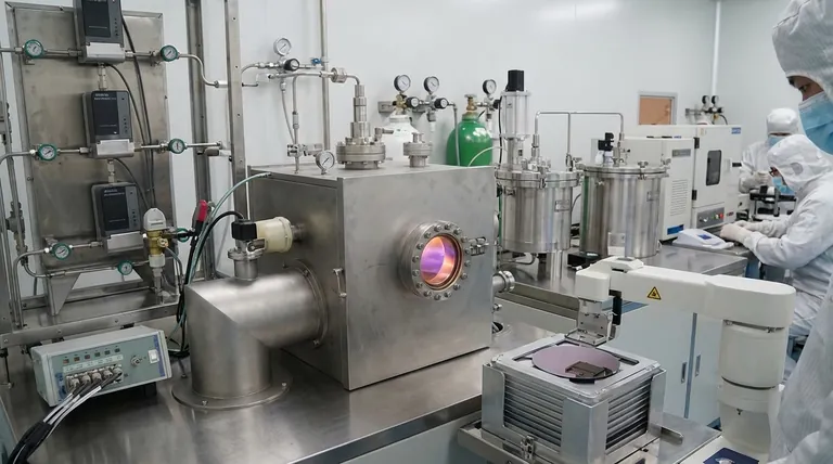
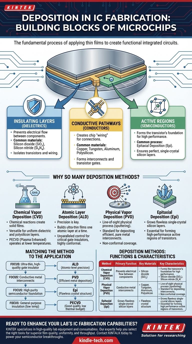
In integrated circuit (IC) fabrication, deposition is the fundamental process used to apply thin films of various materials onto a silicon wafer. These carefully controlled layers are not just coatings; they are the essential building blocks for creating the functional components of a microchip, serving as conductors, insulators, and semiconductors that form every transistor and wire.
The core purpose of deposition is to precisely construct the complex, three-dimensional architecture of an IC. It's the "additive" part of manufacturing, where each deposited layer serves a specific electrical or structural function, enabling billions of microscopic components to work together.
The Core Functions of Deposited Layers
Deposition is fundamentally about adding materials that perform three critical roles within a circuit. Each layer is added for a specific purpose that enables the final device to function correctly.
Creating Insulating Layers (Dielectrics)
To build a functional circuit, you must prevent electricity from flowing to the wrong places. Deposition is used to add insulating materials, known as dielectrics, like silicon dioxide (SiO₂) and silicon nitride (Si₃N₄).
These layers isolate conductive components from one another, preventing short circuits. For example, a dielectric film isolates the transistor's gate from the channel below it, and it separates the multiple layers of metal wiring that connect different parts of the chip.
Forming Conductive Pathways (Conductors)
Once transistors are built, they must be connected. Deposition is used to create the chip's "wiring," or interconnects, by depositing conductive materials.
Metals like copper, tungsten, and aluminum are common choices. This process also includes depositing polycrystalline silicon (polysilicon), which is essential for forming the gate of a transistor—the component that switches it on and off.
Building Active Regions (Semiconductors)
The performance of a transistor is determined by the quality of the silicon it's built in. A process called Epitaxial Deposition (Epi) is used to grow a perfect, single-crystal layer of silicon on top of the starting wafer.
This flawless layer, free of impurities and defects, becomes the active region where the transistor operates, ensuring optimal electrical properties and high performance.
Why So Many Deposition Methods?
The variety of deposition technologies, from CVD to PVD to ALD, exists because no single method is perfect for every application. The choice of technique depends on the material being deposited, the required film quality, and the temperature sensitivity of the existing structures on the wafer.
Chemical Vapor Deposition (CVD)
CVD encompasses a family of techniques (LPCVD, PECVD, APCVD) that use chemical reactions between precursor gases to form a solid film on the wafer's surface.
This method is highly versatile and is a workhorse for creating high-quality, uniform dielectric and polysilicon layers. Plasma Enhanced CVD (PECVD) is particularly valuable because it can operate at lower temperatures, preventing damage to previously built layers.
Atomic Layer Deposition (ALD)
For the most critical components, like the ultra-thin gate insulator in a modern transistor, precision is everything. Atomic Layer Deposition (ALD) provides this by building films one single atomic layer at a time.
While slower than other methods, ALD offers unparalleled control over thickness and uniformity, which is absolutely essential as device features shrink to the nanometer scale.
Physical Vapor Deposition (PVD)
Unlike the chemical reactions of CVD, Physical Vapor Deposition (PVD) is a line-of-sight physical process, often called sputtering. In PVD, a target material is bombarded with ions, ejecting atoms that then land on and coat the wafer.
PVD is the standard method for depositing the metal layers used for interconnects because it is a reliable and efficient way to lay down films of pure metals.
Understanding the Trade-offs
Choosing a deposition method always involves balancing competing requirements. An engineer must consider the geometry of the structure, the device's thermal limits, and the desired quality of the film.
Conformal vs. Non-Conformal Coverage
Some processes, like ALD and LPCVD, produce highly conformal films, meaning they coat the tops, sides, and bottoms of complex 3D structures with a perfectly uniform thickness.
In contrast, PVD is a line-of-sight process and is non-conformal. It can struggle to evenly coat the bottom and sidewalls of deep, narrow trenches, which can be a limitation for certain applications.
Thermal Budget Constraints
Each process step has a thermal budget—a limit on the temperature and time the wafer can be exposed to without damaging structures already fabricated.
High-temperature processes like LPCVD must be used early in the manufacturing flow. Later steps rely on lower-temperature methods like PECVD and PVD to avoid ruining the delicate transistor structures underneath.
Film Quality vs. Throughput
There is often a direct trade-off between the perfection of the deposited film and the speed of the process.
ALD produces near-perfect films but is very slow, making it suitable only for the most critical, thinnest layers. Conversely, other methods may offer higher throughput (more wafers per hour) at the cost of slightly lower film quality, which is acceptable for less critical layers.
Matching the Method to the Application
The right deposition technique is selected based on the specific function of the layer being created.
- If your primary focus is an ultra-thin, high-quality gate insulator: Atomic Layer Deposition (ALD) is the necessary choice for its atomic-level precision.
- If your primary focus is depositing conductive metal interconnects: Physical Vapor Deposition (PVD) is the standard workhorse for its efficiency in metal deposition.
- If your primary focus is a high-purity semiconductor foundation: Epitaxial Deposition (Epi) is used to create the flawless crystal structure needed for high-performance transistors.
- If your primary focus is general-purpose insulation between metal layers: Plasma Enhanced Chemical Vapor Deposition (PECVD) is often used for its good quality at manufacturing-friendly low temperatures.
Ultimately, deposition is the master craft of IC fabrication, enabling the precise, layer-by-layer construction that turns a simple silicon wafer into a powerful processor.
Summary Table:
| Deposition Method | Primary Function | Key Materials | Key Characteristics |
|---|---|---|---|
| Chemical Vapor Deposition (CVD) | Dielectric & Polysilicon Layers | SiO₂, Si₃N₄, Polysilicon | Versatile, uniform films |
| Plasma Enhanced CVD (PECVD) | Low-Temp Insulation | SiO₂, Si₃N₄ | Low thermal budget, good conformity |
| Atomic Layer Deposition (ALD) | Ultra-thin Gate Insulators | High-k dielectrics | Atomic-level precision, high conformity |
| Physical Vapor Deposition (PVD) | Metal Interconnects | Copper, Aluminum, Tungsten | Efficient metal deposition, line-of-sight |
| Epitaxial Deposition (Epi) | High-quality Semiconductor Base | Single-crystal Silicon | Flawless crystal structure for transistors |
Ready to enhance your lab's IC fabrication capabilities? The precision and quality of your deposition processes are critical to your success. KINTEK specializes in high-quality lab equipment and consumables for all your deposition needs, from research to production. Our experts can help you select the right tools to achieve superior film quality, uniformity, and throughput.
Contact KINTALK today to discuss how our solutions can power your next breakthrough in semiconductor technology.
Visual Guide
Related Products
- RF PECVD System Radio Frequency Plasma-Enhanced Chemical Vapor Deposition RF PECVD
- Evaporation Boat for Organic Matter
- Thin-Layer Spectral Electrolysis Electrochemical Cell
- Side Window Optical Electrolytic Electrochemical Cell
- Reference Electrode Calomel Silver Chloride Mercury Sulfate for Laboratory Use
People Also Ask
- What is an example of PECVD? RF-PECVD for High-Quality Thin Film Deposition
- What is plasma CVD? Unlock Low-Temperature Thin Film Deposition for Sensitive Materials
- What is the role of RF-PECVD in VFG preparation? Mastering Vertical Growth and Surface Functionality
- What is plasma chemical vapor deposition? A Low-Temperature Thin Film Coating Solution
- How does Radio Frequency Enhanced Plasma Chemical Vapour Deposition (RF-PECVD) work? Learn the Core Principles


