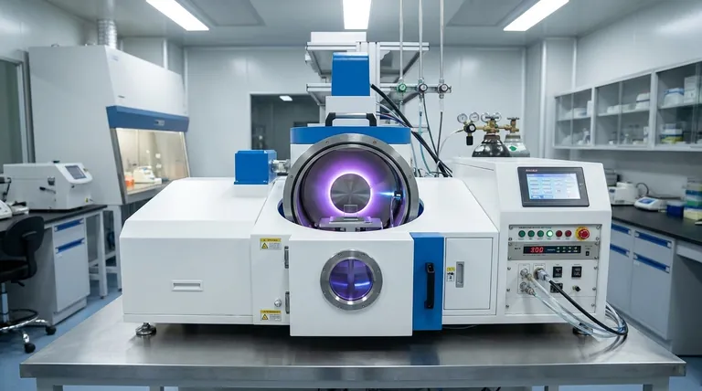
At its core, magnetron sputtering is a highly controlled physical vapor deposition (PVD) process used to create ultra-thin films. It functions by creating a plasma from an inert gas, using ions from that plasma to bombard a source material (the "target"), and depositing the dislodged atoms onto a substrate to form a coating. The defining feature is the use of a magnetic field to dramatically increase the efficiency of this process.
The key to magnetron sputtering is its efficiency. By using a magnetic field to trap electrons near the target, the process creates a dense, self-sustaining plasma that dramatically increases the rate at which atoms are sputtered and deposited, enabling high-quality film growth at lower pressures.
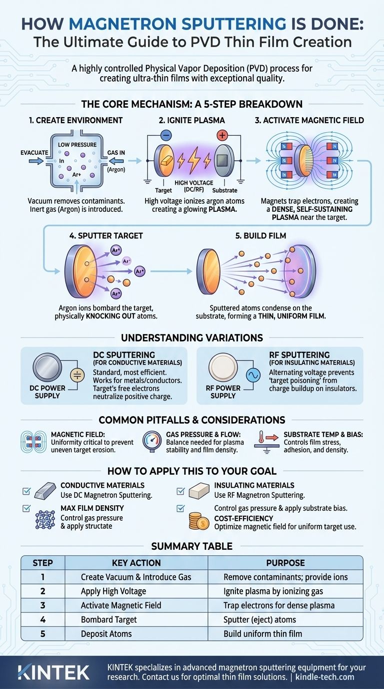
The Core Mechanism: A Step-by-Step Breakdown
To truly understand how magnetron sputtering works, it's best to break it down into its fundamental sequence of events, from the initial vacuum to the final film formation.
Step 1: Creating the Environment
The entire process occurs within a vacuum chamber. First, the chamber is evacuated to a very low pressure to remove contaminants like oxygen and water vapor.
An inert gas, most commonly argon, is then introduced into the chamber, raising the pressure slightly to a stable, controlled level. This gas provides the atoms that will be ionized to create the plasma.
Step 2: Igniting the Plasma
Two electrodes are present in the chamber: a cathode, where the material to be deposited (the target) is mounted, and an anode, which often serves as the holder for the item to be coated (the substrate).
A high negative voltage, typically several hundred volts, is applied to the target. This strong electric field accelerates free electrons and strips electrons from some of the argon atoms, creating a plasma—a glowing, ionized gas consisting of positive argon ions, electrons, and neutral argon atoms.
Step 3: The Role of the Magnetic Field
This is the "magnetron" part of the technique. A set of powerful permanent magnets is placed behind the target.
This magnetic field acts as a trap for the light, negatively charged electrons, confining them in a path close to the surface of the target. Without the magnetic field, electrons would quickly be lost to the chamber walls or anode.
By trapping the electrons, their path length is greatly increased, which massively raises the probability of them colliding with and ionizing neutral argon atoms. This creates a much denser, more intense plasma precisely where it is needed—right in front of the target.
Step 4: Sputtering the Target
The negatively charged target powerfully attracts the positively charged argon ions from the dense plasma.
These ions accelerate toward and collide with the target at high energy. This bombardment is like a microscopic sandblasting process, transferring kinetic energy that physically knocks out, or "sputters," atoms from the target material.
Step 5: Building the Film
The sputtered atoms are ejected from the target as neutral particles. They travel in a straight line through the low-pressure chamber until they strike a surface.
When these atoms land on the substrate, they condense and stick, gradually building up a thin, uniform film layer by layer.
Understanding the Variations
Not all materials can be sputtered with the same method. The electrical conductivity of the target material dictates which type of power supply is required.
DC Sputtering: For Conductive Materials
Direct Current (DC) sputtering is the standard and most efficient method. It uses a constant negative voltage on the target.
This works perfectly for conductive targets (like most metals and transparent conductive oxides) because any positive charge from ion bombardment is immediately neutralized by the target's free electrons.
RF Sputtering: For Insulating Materials
If you try to use DC sputtering on an insulating (dielectric) target, such as a ceramic or oxide, a problem arises. Positive charge from the argon ions quickly builds up on the target's surface.
This buildup, known as "target poisoning," effectively neutralizes the negative voltage, repels incoming argon ions, and shuts down the sputtering process.
Radio Frequency (RF) sputtering solves this by alternating the voltage at high frequency. During the negative cycle, sputtering occurs as normal. During the brief positive cycle, the target attracts electrons from the plasma, which neutralizes the positive charge built up on its surface, allowing the process to continue.
Common Pitfalls and Considerations
Achieving a high-quality film requires careful control over several variables. Simply running the process is not enough.
Magnetic Field Strength and Uniformity
The design of the magnet array behind the target is critical. A non-uniform magnetic field will lead to uneven plasma density, causing the target to erode in a specific pattern (a "racetrack"). This results in poor target material utilization and can affect the uniformity of the deposited film.
Gas Pressure and Flow
The pressure of the inert gas is a delicate balance. If it's too high, sputtered atoms will collide with too many gas atoms before reaching the substrate, losing energy and reducing the film's density. If it's too low, the plasma may be unstable or difficult to sustain, lowering the deposition rate.
Substrate Temperature and Bias
Controlling the substrate temperature is crucial for managing film stress, grain structure, and adhesion. In some cases, a small negative voltage (bias) is also applied to the substrate to attract some ions, providing a slight bombardment that can improve the density and quality of the growing film.
How to Apply This to Your Goal
Your choice of sputtering technique depends entirely on the material you need to deposit and your desired film properties.
- If your primary focus is depositing conductive materials (like metals): DC magnetron sputtering is the most efficient, fastest, and cost-effective method.
- If your primary focus is depositing insulating materials (like ceramics or oxides): RF magnetron sputtering is required to prevent positive charge buildup on the target.
- If your primary focus is achieving maximum film density and quality: You must precisely control gas pressure and consider applying a bias voltage to your substrate during deposition.
- If your primary focus is cost-efficiency and material yield: Optimizing the magnetron's magnetic field configuration to ensure uniform target erosion is the most critical factor.
Ultimately, magnetron sputtering provides an exceptional level of control over film properties, making it one of the most versatile and widely used deposition technologies available.
Summary Table:
| Step | Key Action | Purpose |
|---|---|---|
| 1 | Create Vacuum & Introduce Gas | Remove contaminants; provide ions for plasma |
| 2 | Apply High Voltage to Target | Ignite plasma by ionizing inert gas (e.g., Argon) |
| 3 | Activate Magnetic Field | Trap electrons to create dense, efficient plasma |
| 4 | Bombard Target with Ions | Sputter (eject) atoms from the target material |
| 5 | Deposit Atoms on Substrate | Build a uniform, high-quality thin film layer by layer |
Ready to achieve precise, high-quality thin films in your lab? KINTEK specializes in advanced magnetron sputtering equipment and consumables for laboratory needs. Whether you're working with conductive metals or insulating ceramics, our solutions ensure optimal deposition rates, film uniformity, and material utilization. Contact our experts today to discuss how we can enhance your thin film research and production.
Visual Guide
Related Products
- Microwave Plasma Chemical Vapor Deposition MPCVD Machine System Reactor for Lab and Diamond Growth
- Chemical Vapor Deposition CVD Equipment System Chamber Slide PECVD Tube Furnace with Liquid Gasifier PECVD Machine
- Molybdenum Tungsten Tantalum Special Shape Evaporation Boat
- Inclined Rotary Plasma Enhanced Chemical Vapor Deposition PECVD Equipment Tube Furnace Machine
- Inclined Rotary Plasma Enhanced Chemical Vapor Deposition PECVD Equipment Tube Furnace Machine
People Also Ask
- How are CVD diamonds created? Discover the Science of Lab-Grown Diamond Precision
- How is a diamond formed from CVD? The Science of Growing Diamonds Atom by Atom
- What are the primary advantages of the CVD method for growing diamonds? Engineering High-Purity Gems and Components
- Why is argon-rich gas phase chemistry used for UNCD growth? Unlock Precision Nano-Diamond Synthesis
- What is microwave plasma chemical vapor deposition? A Guide to High-Purity Diamond Film Growth