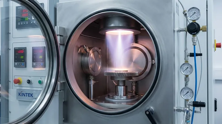
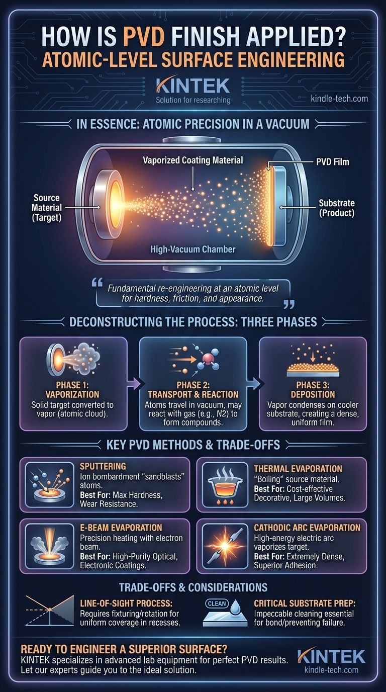
In essence, applying a PVD finish involves placing a product into a high-vacuum chamber and depositing a vaporized coating material onto its surface, one atom at a time. The source material is turned into a vapor through methods like sputtering or heating, which then travels through the vacuum and condenses onto the target object, forming an extremely thin, durable, and precisely controlled film.
The core principle of Physical Vapor Deposition (PVD) is not merely to coat an object, but to fundamentally re-engineer its surface at an atomic level. This precision is what allows for significant improvements in hardness, friction, and appearance using only a microscopic layer of material.
Deconstructing the PVD Process
To truly understand how PVD is applied, it's best to break it down into its fundamental stages. Each step is meticulously controlled to achieve the desired outcome.
The Vacuum Environment is Essential
The entire process takes place in a chamber pumped to a very high vacuum. This is critical for two reasons: it removes any atmospheric gases that could contaminate the coating, and it allows the vaporized atoms to travel directly to the substrate without colliding with air molecules.
Phase 1: Vaporization (Creating the Atomic Cloud)
The first step is to convert a solid source material, known as the "target," into a vapor. This is the defining stage of the process, and several methods exist to accomplish it. The goal is to liberate individual atoms or molecules from the solid target.
Phase 2: Transportation and Reaction
Once vaporized, these atoms travel through the vacuum chamber. During this transit, a reactive gas (like nitrogen, oxygen, or methane) can be introduced into the chamber. This gas reacts with the metal atoms to form a specific compound coating, such as titanium nitride (for a gold color and hardness) or chromium nitride.
Phase 3: Deposition (Building the Film)
When the vaporized atoms reach the cooler surface of the product (the "substrate"), they condense and form a thin, highly adherent film. Because this happens on an atom-by-atom basis, the resulting coating is exceptionally dense and uniform, capable of replicating even the finest surface textures.
Key PVD Methods Explained
The primary difference between PVD techniques lies in how the solid material is vaporized in Phase 1. The chosen method depends on the coating material and the desired properties of the final finish.
Sputtering (The Atomic "Sandblasting")
In sputtering, the chamber is filled with a small amount of an inert gas, typically argon, which is then ionized to create plasma. These high-energy ions are accelerated toward the target material, bombarding it with such force that they "knock off" or sputter individual atoms, which then deposit onto the substrate.
Thermal Evaporation (The "Boiling" Method)
This method involves heating the source material in the vacuum until it evaporates, much like boiling water turns to steam. The material is often held in a container that is heated by an electrical resistive element. It is a simpler, cost-effective method suitable for certain materials like gold.
Electron-Beam Evaporation (The Precision Heating Method)
A more advanced form of evaporation, this technique uses a high-energy beam of electrons to heat the target material in a very localized spot. This allows for the evaporation of materials with very high melting points and provides excellent control over the purity of the coating.
Cathodic Arc Evaporation (The High-Energy Spark)
In this method, a high-current, low-voltage electric arc is struck on the surface of the target. The intense energy of the arc spot vaporizes the material and creates a highly ionized vapor. This high level of ionization results in extremely dense coatings with superior adhesion.
Understanding the Trade-offs and Considerations
While powerful, PVD is not a universal solution. Understanding its limitations is key to using it effectively.
It is a Line-of-Sight Process
PVD atoms travel in a relatively straight line from the source to the substrate. This means that surfaces that are "hidden" or in deep recesses may not receive a uniform coating. Fixturing and part rotation are often used to mitigate this, but it remains a fundamental constraint.
Substrate Preparation is Critical
The final coating is only as good as its bond to the surface. The substrate must be impeccably clean and free of any oils, oxides, or contaminants. Improper cleaning is a primary cause of coating failure, such as flaking or peeling.
Method Determines Film Properties
The choice between sputtering and evaporation is not arbitrary. Sputtering often produces denser films with better adhesion due to the higher energy of the depositing atoms. Evaporation, however, can achieve higher deposition rates and is often preferred for high-purity optical or electronic coatings.
Making the Right Choice for Your Product
Your goal dictates the best approach to PVD. The process can be tailored for performance, aesthetics, or a balance of both.
- If your primary focus is maximum hardness and wear resistance: Sputtering or Arc Evaporation are generally preferred as they create the densest, most durable films.
- If your primary focus is a high-purity decorative or optical finish: Electron-Beam Evaporation provides excellent control over material purity and is ideal for sensitive applications.
- If your primary focus is a cost-effective metallic finish on a large volume of parts: Simpler methods like Thermal Evaporation or basic DC Sputtering can provide excellent cosmetic results without the cost of more complex processes.
By understanding PVD as a toolkit for atomic-level surface engineering, you can select the precise method to add significant value and performance to your product.
Summary Table:
| PVD Method | How It Works | Best For |
|---|---|---|
| Sputtering | Atoms are "knocked off" a target by ion bombardment. | Maximum hardness, wear resistance, dense films. |
| Thermal Evaporation | Source material is heated until it evaporates. | Cost-effective decorative finishes on large volumes. |
| Electron-Beam Evaporation | A high-energy electron beam precisely heats the target. | High-purity optical, electronic, or decorative coatings. |
| Cathodic Arc Evaporation | An electric arc vaporizes the target, creating a highly ionized vapor. | Extremely dense coatings with superior adhesion. |
Ready to Engineer a Superior Surface for Your Product?
The precise, atom-by-atom control of PVD coating can fundamentally enhance your product's hardness, reduce friction, and create stunning, durable finishes. Choosing the right method—from sputtering for maximum durability to evaporation for high-purity aesthetics—is critical to your success.
KINTEK specializes in advanced lab equipment and consumables for surface engineering, helping laboratories and manufacturers achieve perfect results. Let our experts guide you to the ideal PVD solution for your specific application.
Contact KINTEK today to discuss how PVD coating can add value and performance to your product.
Visual Guide
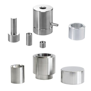
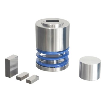
Related Products
- RF PECVD System Radio Frequency Plasma-Enhanced Chemical Vapor Deposition RF PECVD
- Molybdenum Tungsten Tantalum Evaporation Boat for High Temperature Applications
- Chemical Vapor Deposition CVD Equipment System Chamber Slide PECVD Tube Furnace with Liquid Gasifier PECVD Machine
- Tungsten Evaporation Boat for Thin Film Deposition
- VHP Sterilization Equipment Hydrogen Peroxide H2O2 Space Sterilizer
People Also Ask
- What are the applications of PECVD? Essential for Semiconductors, MEMS, and Solar Cells
- Why is PECVD environment friendly? Understanding the Eco-Friendly Benefits of Plasma-Enhanced Coating
- What is plasma activated chemical vapour deposition method? A Low-Temperature Solution for Advanced Coatings
- What are the benefits of PECVD? Achieve Superior Low-Temperature Thin Film Deposition
- What is the principle of plasma enhanced chemical vapor deposition? Achieve Low-Temperature Thin Film Deposition