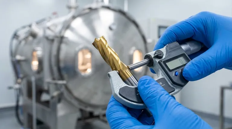
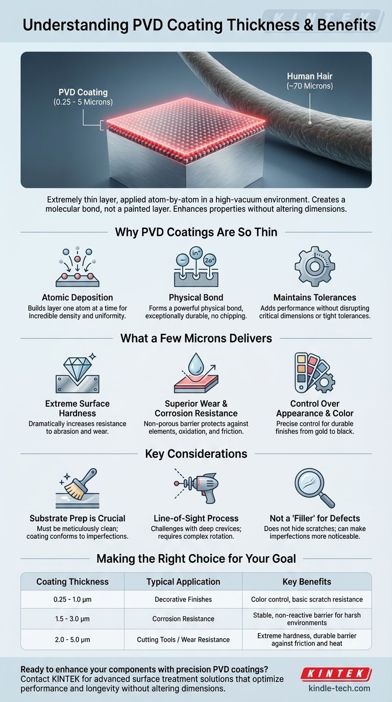
In most applications, a PVD coating is between 0.25 and 5 microns (μm) thick. This extremely thin layer is applied atom-by-atom in a high-vacuum environment, creating a surface that is molecularly bonded to the underlying material, not simply painted on top. The result is a finish that fundamentally enhances the part's properties.
The critical takeaway is that PVD coatings are intentionally microscopic. Their value comes not from thickness, but from adding extreme surface hardness, lubricity, and corrosion resistance without altering the fundamental dimensions or tight tolerances of the component.
Why PVD Coatings Are So Thin
The thinness of a Physical Vapor Deposition (PVD) coating is not a limitation but its defining characteristic. The process is engineered at a molecular level to achieve specific performance goals that a thicker coating could not.
The Atomic Deposition Process
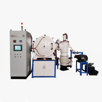
PVD is a thin-film deposition technique. Inside a vacuum chamber, a solid source material (like titanium or zirconium) is vaporized into a plasma of individual atoms or molecules.
These energized particles then travel and condense onto the target component, building a new surface layer one atom at a time. This atomic-level precision creates an incredibly dense, uniform, and well-adhered coating.
A Physical Bond, Not a Layer of Paint
Unlike traditional plating or painting which creates a distinct mechanical layer, PVD forms a powerful physical bond.
The high-energy ions embed themselves into the substrate's surface, creating an interlocking transition layer. This is why PVD coatings are exceptionally durable and do not chip or flake easily.
Maintaining Critical Tolerances
For precision components like cutting tools, engine parts, or medical implants, even a few extra microns can disrupt function.
PVD provides a solution by adding significant performance enhancements without meaningfully changing the part's dimensions. It improves the part without compromising its engineered fit and function.
What a Few Microns of PVD Delivers
That microscopic layer, often less than a tenth the thickness of a human hair, imparts dramatic improvements to the substrate's surface.
Extreme Surface Hardness
The primary benefit of many PVD coatings is a radical increase in surface hardness.
A thin layer of a very hard ceramic compound, like Titanium Nitride (TiN), acts as a protective shield for the softer metal underneath, dramatically increasing its resistance to abrasion and wear.
Superior Wear and Corrosion Resistance
The PVD process creates a chemically stable and non-porous layer. This dense film acts as an effective barrier, protecting the substrate from corrosive elements, oxidation, and friction.
The result is a longer lifespan for components operating in harsh environments.
Control Over Appearance and Color
The PVD process allows for precise control over the final appearance.
By introducing reactive gases like nitrogen or acetylene into the vacuum chamber, different compounds are formed on the surface, each with a unique, durable color. This allows for finishes ranging from gold and rose gold to graphite and black.
Understanding the Trade-offs and Considerations
While powerful, the PVD process has specific requirements that are critical for success. Understanding these ensures you are using the technology correctly.
Substrate Preparation is Crucial
A PVD coating is only as good as the surface it is applied to. The coating is so thin that it will perfectly conform to the underlying topography.
Any surface imperfections, oils, or contaminants must be meticulously removed before coating. A perfectly smooth, clean surface is essential for optimal adhesion and performance.
It is a Line-of-Sight Process
The vaporized coating material travels in a straight line from the source to the part.
Coating complex internal geometries or deep crevices can be challenging. This is managed through sophisticated rotation and positioning of the parts inside the chamber, but it remains a key consideration for part design.
Not a "Filler" for Surface Defects
Unlike thick paint or powder coating, PVD will not hide or fill in scratches, tool marks, or other surface defects.
In fact, the high-gloss nature of many PVD finishes can make these underlying imperfections more noticeable. The initial surface finish must be exactly what you want the final finish to be.
Making the Right Choice for Your Goal
The ideal coating thickness is determined entirely by the application's primary demand.
- If your primary focus is a decorative finish: A thinner coating (typically 0.25 to 1.0 micron) is often sufficient to achieve the desired color and provide basic scratch resistance.
- If your primary focus is wear resistance on cutting tools: A thicker, often multi-layered, coating (typically 2.0 to 5.0 microns) is required to provide a durable barrier against extreme friction and heat.
- If your primary focus is corrosion resistance or biocompatibility: A mid-range thickness (typically 1.5 to 3.0 microns) of a specific inert material is chosen to create a stable, non-reactive surface barrier.
Ultimately, the microscopic thickness of a PVD coating is a deliberate engineering feature that enhances performance without compromising precision.
Summary Table:
| Coating Thickness (Microns) | Typical Application | Key Benefits |
|---|---|---|
| 0.25 - 1.0 μm | Decorative Finishes | Color control, basic scratch resistance |
| 1.5 - 3.0 μm | Corrosion Resistance | Stable, non-reactive barrier for harsh environments |
| 2.0 - 5.0 μm | Cutting Tools / Wear Resistance | Extreme hardness, durable barrier against friction and heat |
Ready to enhance your components with precision PVD coatings?
At KINTEK, we specialize in advanced lab equipment and consumables for surface treatment applications. Our expertise ensures your parts receive the optimal coating thickness for extreme hardness, wear resistance, and corrosion protection—without altering critical dimensions.
Contact us today to discuss how our solutions can improve your product's performance and longevity.
Visual Guide
Related Products
- Graphite Vacuum Continuous Graphitization Furnace
- Vacuum Heat Treat and Molybdenum Wire Sintering Furnace for Vacuum Sintering
- 2200 ℃ Graphite Vacuum Heat Treat Furnace
- High Pressure Laboratory Vacuum Tube Furnace Quartz Tubular Furnace
- Small Vacuum Heat Treat and Tungsten Wire Sintering Furnace
People Also Ask
- Is graphite good for high temperature? Unlock Its Full Potential in Controlled Atmospheres
- How well does graphite transfer heat? Unlock Superior Thermal Management for Your Electronics
- What is the graphite furnace used for? Achieve Extreme Heat Up to 3000°C in a Controlled Environment
- Why can graphite withstand heat? Unlocking Its Extreme Thermal Stability for Your Lab
- What is the maximum working temperature of graphite? Unlock High-Temp Performance with the Right Atmosphere