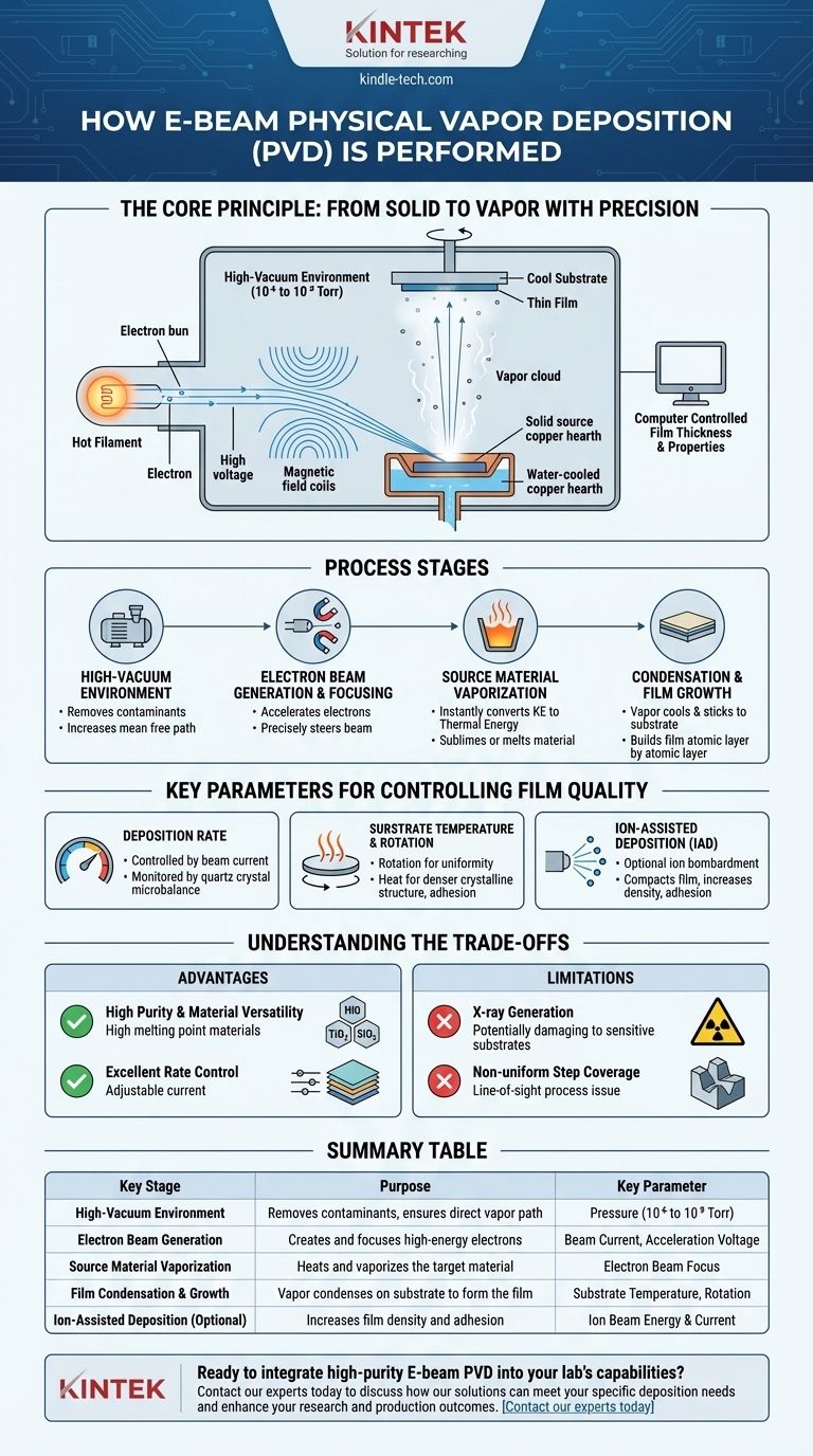
In essence, Electron Beam Physical Vapor Deposition (E-beam PVD) is a high-vacuum process that uses a focused beam of high-energy electrons to heat and vaporize a source material. This vapor then travels through the vacuum and condenses onto a cooler substrate, forming a thin, precisely controlled film. The entire process is managed by computer to control film thickness, uniformity, and material properties.
The core principle of E-beam deposition is its ability to transfer immense energy into a very small area. This allows it to vaporize even materials with extremely high melting points, offering a level of material versatility and purity that is difficult to achieve with other methods.
The Core Principle: From Solid to Vapor with Precision
E-beam PVD is a line-of-sight deposition technique performed inside a high-vacuum chamber. Each stage of the process is critical for achieving a high-quality, uniform thin film.
The High-Vacuum Environment
First, the deposition chamber is pumped down to a high vacuum, typically between 10⁻⁶ and 10⁻⁹ Torr. This is crucial for two reasons: it removes atmospheric gases that could contaminate the film, and it increases the mean free path—the average distance an atom can travel before colliding with another gas molecule. A long mean free path ensures the vaporized material travels directly to the substrate without scattering.
Generating and Focusing the Electron Beam
An electron beam is generated from a hot filament, typically made of tungsten. A high voltage (several kilovolts) accelerates these electrons toward the source material. Magnetic fields are used to precisely bend and focus the electron beam, steering it to strike a specific spot within a water-cooled copper hearth or crucible holding the source material.
Vaporizing the Source Material
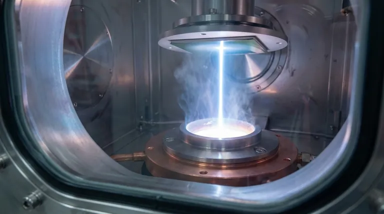
Upon impact, the kinetic energy of the electrons is instantly converted into intense thermal energy. This localized heating is so powerful it can cause the source material to sublimate (go from solid to gas) or melt and then evaporate. Because the crucible itself is water-cooled, only the targeted material gets hot, which minimizes contamination from the crucible.
Condensation and Film Growth
The resulting vapor cloud travels in a straight line from the source to the substrate, which is positioned above. When the hot vapor atoms or molecules strike the relatively cool surface of the substrate, they lose their energy, condense, and stick to the surface. This builds up the desired film, one atomic layer at a time.
Key Parameters for Controlling Film Quality
The final properties of the film are not accidental; they are dictated by careful control over several key process parameters.
Deposition Rate
The deposition rate is directly controlled by the electron beam's current. A higher current delivers more energy, increasing the rate of evaporation and, consequently, how quickly the film grows. This rate is monitored in real-time, often with a quartz crystal microbalance, allowing for precise control over the final film thickness.
Substrate Temperature and Rotation
The substrate is often rotated to ensure the depositing vapor coats it uniformly from all angles. The substrate's temperature is also a critical parameter. Heating the substrate can provide surface atoms with more energy to arrange themselves into a denser, more ordered crystalline structure and improves film adhesion.
Ion-Assisted Deposition (IAD)
To create exceptionally dense and durable films, the process can be enhanced with an ion source. This source bombards the growing film with a beam of low-energy ions (such as argon). This bombardment acts like an atomic-scale hammer, compacting the film, increasing its density, improving adhesion, and reducing internal stress.
Understanding the Trade-offs
Like any technology, E-beam PVD has distinct advantages and limitations that make it suitable for specific applications.
Advantage: High Purity and Material Versatility
The primary advantage of E-beam is its ability to deposit materials with very high melting points, such as titanium, tungsten, and ceramic oxides like TiO₂ or SiO₂. The water-cooled hearth prevents contamination that can occur in other thermal evaporation methods.
Advantage: Excellent Rate Control
The electron beam current can be adjusted almost instantaneously. This provides dynamic and precise control over the deposition rate, which is critical for fabricating complex structures like multi-layer optical coatings.
Limitation: X-ray Generation
The impact of high-energy electrons on the source material can generate X-rays. While the chamber is shielded, this radiation can potentially damage sensitive substrates, such as certain electronic components or polymers.
Limitation: Non-uniform Step Coverage
Because E-beam is a line-of-sight process, it can struggle to uniformly coat complex, three-dimensional surfaces with sharp edges or deep trenches. The "shadows" cast by these features result in thinner or non-existent coating in those areas.
Making the Right Choice for Your Goal
Selecting E-beam PVD depends entirely on your material requirements and application demands.
- If your primary focus is depositing high-purity optical films or refractory metals: E-beam is an ideal choice due to its high-energy source and clean evaporation environment.
- If your primary focus is creating complex, multi-layer stacks with precise thickness: The excellent rate control of E-beam makes it a superior technology for this purpose.
- If your primary focus is producing dense, environmentally robust coatings: Combining E-beam with Ion-Assisted Deposition (IAD) will yield superior film quality and durability.
- If your primary focus is coating complex 3D parts with high uniformity: You should consider alternative PVD methods like sputtering, which is less directional and provides better step coverage.
Ultimately, electron beam deposition is a powerful and versatile tool for creating high-performance thin films when precision, purity, and material flexibility are paramount.
Summary Table:
| Key Stage | Purpose | Key Parameter |
|---|---|---|
| High-Vacuum Environment | Removes contaminants, ensures direct vapor path | Pressure (10⁻⁶ to 10⁻⁹ Torr) |
| Electron Beam Generation | Creates and focuses high-energy electrons | Beam Current, Acceleration Voltage |
| Source Material Vaporization | Heats and vaporizes the target material | Electron Beam Focus |
| Film Condensation & Growth | Vapor condenses on substrate to form the film | Substrate Temperature, Rotation |
| Ion-Assisted Deposition (Optional) | Increases film density and adhesion | Ion Beam Energy & Current |
Ready to integrate high-purity E-beam PVD into your lab's capabilities? KINTEK specializes in advanced lab equipment, including electron beam evaporation systems, to help you achieve precise, high-performance thin films for optics, electronics, and more. Contact our experts today to discuss how our solutions can meet your specific deposition needs and enhance your research and production outcomes.
Visual Guide
Related Products
- Electron Beam Evaporation Coating Tungsten Crucible and Molybdenum Crucible for High Temperature Applications
- Electron Beam Evaporation Coating Oxygen-Free Copper Crucible and Evaporation Boat
- Electron Beam Evaporation Coating Gold Plating Tungsten Molybdenum Crucible for Evaporation
- Electron Beam Evaporation Coating Conductive Boron Nitride Crucible BN Crucible
- High Purity Pure Graphite Crucible for Electron Beam Evaporation
People Also Ask
- What are the applications of e-beam evaporation? Achieve High-Purity Coatings for Optics & Electronics
- What is the container that holds the metal source material called in e-beam evaporation? Ensure Purity and Quality in Your Thin-Film Deposition
- What is the process of e-beam coating? Achieve High-Purity, Precise Thin Films for Your Lab
- What is the current of e-beam evaporation? A Guide to High-Purity Thin Film Deposition
- What is the temperature of e-beam evaporation? Mastering the Two-Zone Thermal Process for Precision Films


