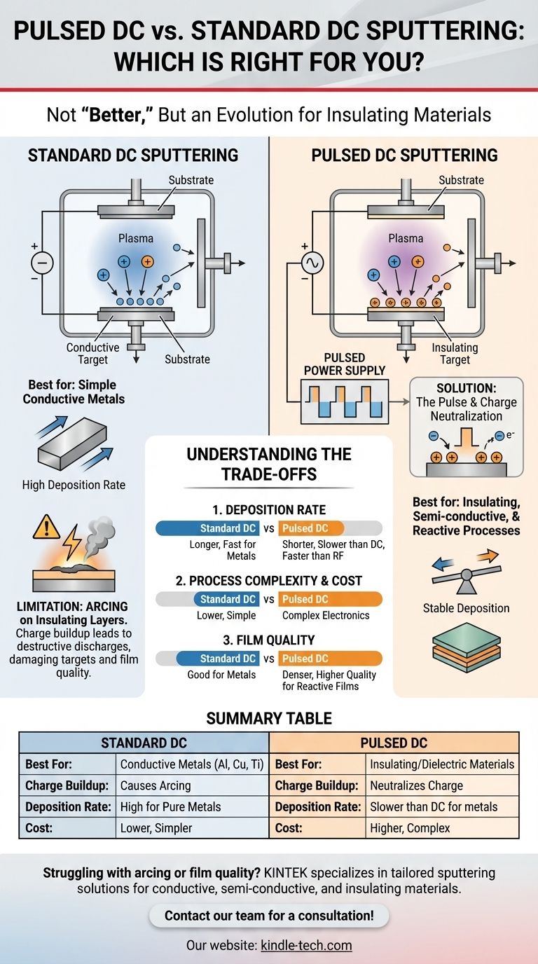
To be direct, pulsed DC sputtering is not inherently "better" than standard DC sputtering. Rather, it is an advanced evolution designed to solve a critical limitation of the standard DC method. The choice between them depends entirely on the type of material you are depositing. For simple conductive metals, standard DC is often faster and more cost-effective. For insulating or semi-conductive materials, pulsed DC is essential for a stable process.
The core difference comes down to managing electrical charge. Standard DC sputtering is the go-to for conductive targets but fails when insulating layers form, causing destructive arcing. Pulsed DC sputtering solves this arcing problem, expanding the process to a much wider range of materials at deposition rates often far exceeding those of RF sputtering.
The Foundation: Understanding Standard DC Sputtering
How It Works
In the simplest terms, standard DC (Direct Current) sputtering involves applying a constant negative voltage to a target material within a vacuum chamber. This creates a plasma, and positive ions from this plasma accelerate towards the negatively charged target, striking it with enough force to eject, or "sputter," atoms. These sputtered atoms then travel and deposit onto your substrate, forming a thin film.
Key Strengths
The primary advantages of standard DC sputtering are its simplicity, high deposition rate, and low cost. The power supplies are relatively inexpensive and easy to control, making it the most economical and efficient method for depositing conductive materials like pure metals and transparent conductive oxides.
The Critical Limitation: Arcing
The process works flawlessly as long as the target material remains electrically conductive. However, if you attempt to sputter an insulating (dielectric) material or use a reactive gas that forms an insulating layer on the target (like oxygen forming an oxide), a major problem arises.
Positive ions from the plasma become trapped on the target's non-conductive surface. This charge buildup eventually reaches a point where it catastrophically discharges in the form of a powerful arc. These arcs can damage the target, the power supply, and destroy the quality of the film being deposited.
The Evolution: How Pulsed DC Solves the Arcing Problem
The Core Mechanism: The Pulse
Pulsed DC sputtering addresses the arcing problem directly. Instead of a constant DC voltage, the power supply delivers the negative voltage in short, high-frequency bursts or pulses (typically in the tens to hundreds of kHz range).
The 'Off' Time is Key
Crucially, between each negative pulse, a brief reverse-polarity (positive) voltage is applied. This short positive pulse attracts electrons from the plasma, which effectively neutralize the positive charge that began accumulating on the target surface during the main sputtering pulse.
The Result: Stable, Arc-Free Deposition
By continuously neutralizing this charge buildup before it can reach a critical point, pulsed DC technology prevents arcing. This makes it possible to reliably sputter dielectric compounds or run reactive sputtering processes for extended periods without instability, bridging the gap between the capabilities of DC and RF systems.
Understanding the Trade-offs
Choosing a technology always involves balancing benefits and drawbacks. Pulsed DC is powerful, but it is not a universal replacement for standard DC.
Deposition Rate
While pulsed DC offers far higher deposition rates than RF for dielectric materials, it is typically slower than standard DC for depositing a pure, conductive metal. The brief "off" time in the duty cycle, while necessary, means less time is spent actively sputtering compared to a continuous DC process at the same peak power.
Process Complexity and Cost
Simplicity is a major advantage of standard DC. The power supplies are straightforward and less expensive. Pulsed DC power supplies are significantly more complex and costly due to the advanced electronics required to generate and control the high-frequency pulses and voltage reversals.
Film Quality and Density
In many reactive sputtering applications (e.g., depositing titanium nitride or aluminum oxide), pulsed DC can produce denser and higher-quality films. The high plasma density achieved during the peak of each pulse can lead to improved film morphology and stoichiometry compared to other methods.
Making the Right Choice for Your Application
Your decision should be guided by your specific material and process goals.
- If your primary focus is cost-effective deposition of pure metals (like aluminum, copper, or titanium): Standard DC sputtering is the superior choice for its unmatched speed, simplicity, and low equipment cost.
- If your primary focus is reactive sputtering (depositing oxides, nitrides) or sputtering semi-conductive materials: Pulsed DC sputtering is the essential technology to prevent arcing and ensure a stable, repeatable, and high-rate deposition process.
- If your primary focus is depositing highly insulating materials where deposition rate is not critical: RF sputtering remains a reliable option, but pulsed DC is often preferred in industrial settings for its significant speed advantage.
By understanding the fundamental role of charge buildup and arcing, you can confidently select the sputtering technique that aligns perfectly with your material, budget, and production goals.
Summary Table:
| Feature | Standard DC Sputtering | Pulsed DC Sputtering |
|---|---|---|
| Best For | Conductive metals (Al, Cu, Ti) | Insulating/dielectric materials, reactive processes |
| Charge Buildup | Causes arcing on insulating layers | Neutralizes charge, prevents arcing |
| Deposition Rate | High for pure metals | Slower than DC for metals, but faster than RF for dielectrics |
| Cost & Complexity | Lower cost, simpler power supply | Higher cost, more complex electronics |
| Film Quality | Good for metals | Denser, higher-quality films in reactive processes |
Struggling with arcing or film quality in your sputtering process? KINTEK specializes in lab equipment and consumables, providing tailored sputtering solutions for laboratories working with conductive, semi-conductive, and insulating materials. Our experts can help you choose the right technology—whether standard DC for cost-effective metal deposition or pulsed DC for stable reactive processes—to enhance your thin-film results and lab efficiency. Contact our team today for a consultation!
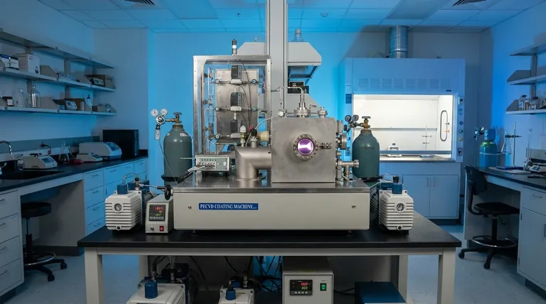
Visual Guide
Related Products
- Laboratory Sterilizer Lab Autoclave Pulsating Vacuum Desktop Steam Sterilizer
- Single Punch Electric Tablet Press Machine Laboratory Powder Tablet Punching TDP Tablet Press
- Laboratory Scientific Electric Heating Blast Drying Oven
- Spark Plasma Sintering Furnace SPS Furnace
- Vibrating Disc Mill Small Laboratory Grinding Machine
People Also Ask
- What is the importance of using a laboratory autoclave in ZSM-5 synthesis? Achieve Perfect Zeolite Crystallization
- Why is a laboratory autoclave necessary for Postgate Medium B (PMB)? Ensure Pure SRB Cultures & Accurate MIC Research
- In what industries and applications are steam sterilizers or autoclaves used? Discover Key Uses Across 4 Major Sectors
- What is an autoclave laboratory equipment? The Ultimate Guide to Steam Sterilization
- What is the primary function of a laboratory sterilization autoclave? Master the Physics of Wet Heat Sterilization