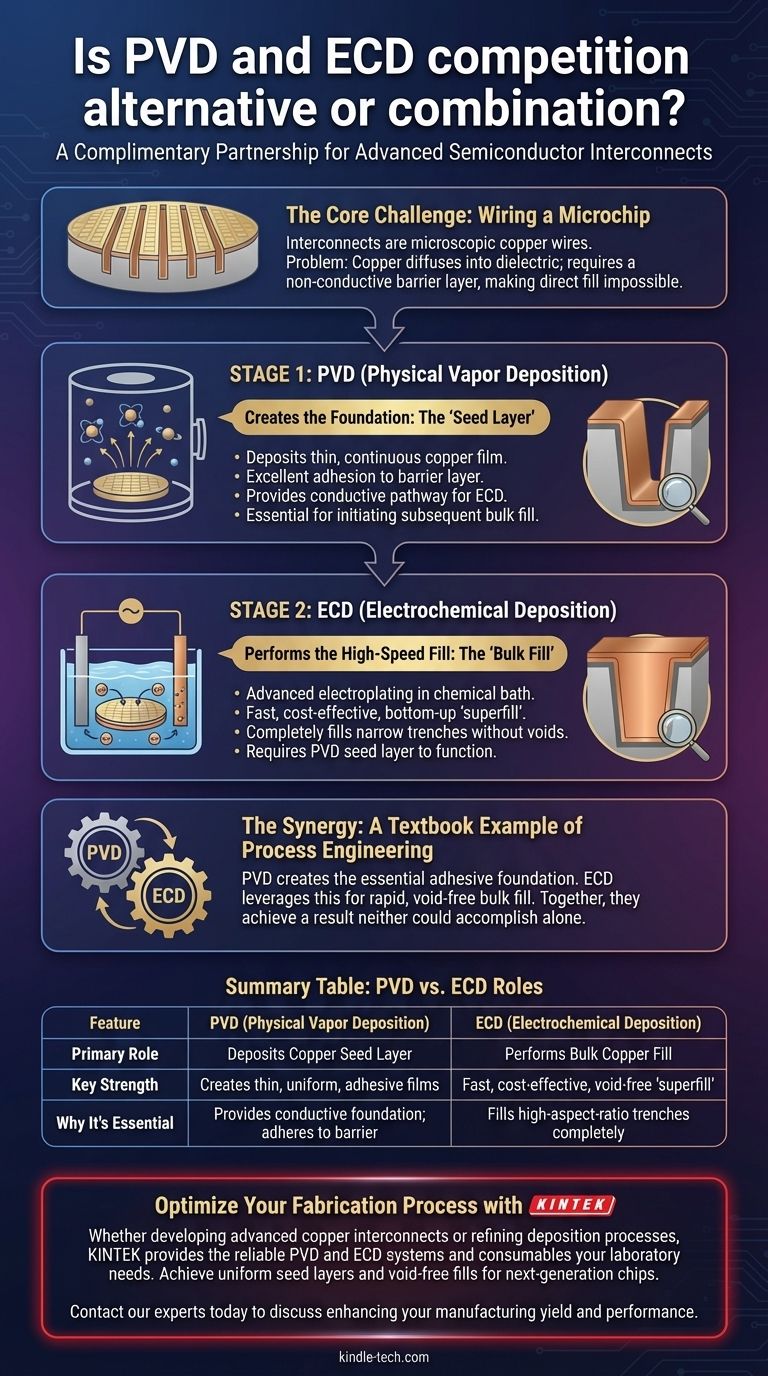
In advanced semiconductor manufacturing, Physical Vapor Deposition (PVD) and Electrochemical Deposition (ECD) are not competitors. They are two complementary stages of a single, highly optimized process. For creating copper interconnects, PVD is used first to create a thin, critical "seed layer," which then enables the subsequent ECD step to perform the fast, high-volume "bulk fill."
The core misunderstanding is to view PVD and ECD as alternatives. In reality, modern chip fabrication depends on their sequential partnership. This combination leverages the unique strengths of each technology to solve a problem that neither could handle effectively on its own.
The Core Challenge: Wiring a Microchip
To understand why this partnership is necessary, we must first understand the fundamental problem: connecting the billions of transistors on a modern processor.
What are Interconnects?
Interconnects are the microscopic copper "wires" that transmit signals and power between transistors and other components on a chip.
As transistors have shrunk, these wires have become incredibly narrow and deep, creating significant manufacturing challenges.
The Problem with Copper
Copper is an excellent conductor, but it has two major flaws in this context. It diffuses into the surrounding insulating material (the dielectric), which can destroy the chip, and it does not adhere well to the common dielectric materials used.
To solve this, a non-conductive barrier layer (typically made of Tantalum or Tantalum Nitride) is first deposited to line the trenches where the wires will be formed. This isolates the copper but creates a new problem: how to fill these non-conductive trenches with copper.
The Role of PVD: Creating the Foundation
The first step in filling the barrier-lined trench is Physical Vapor Deposition.
What is PVD?
PVD is a process where a material is vaporized in a vacuum and deposited atom by atom onto a target surface, like a silicon wafer. In this case, a process called sputtering is used to bombard a copper target, ejecting copper atoms that coat the wafer.
The "Seed Layer" is Essential
The primary strength of PVD is its ability to create an extremely thin, continuous, and highly uniform layer of copper that adheres well to the underlying barrier layer. This is called the seed layer.
This seed layer provides the essential conductive pathway required for the next step in the process.
Why PVD Can't Do the Whole Job
While excellent for thin films, PVD is a relatively slow and expensive process for depositing thick layers. More importantly, as it deposits material line-of-sight, it can create an "overhang" at the top opening of a narrow trench, which may pinch off and create a void or seam during the fill.
The Role of ECD: The High-Speed Fill
Once the PVD seed layer is in place, the wafer moves to an Electrochemical Deposition process.
What is ECD?
ECD is essentially advanced electroplating. The wafer is immersed in a chemical bath rich with copper ions, and an electrical current is applied.
Why ECD Needs a Seed Layer
ECD can only deposit metal onto an already conductive surface. It cannot deposit directly onto the non-conductive barrier layer.
The PVD seed layer provides the necessary conductive "scaffolding" that allows the ECD process to begin plating copper across the entire wafer.
The "Superfill" Advantage
ECD is fast, cost-effective, and has a unique "bottom-up" filling characteristic. Through carefully engineered chemical additives in the bath, deposition occurs faster at the bottom of the trench than at the top.
This superfilling behavior ensures the narrow trenches are filled completely from the bottom up, preventing the formation of the voids and seams that can plague a PVD-only fill.
Understanding the Trade-offs
The choice to use both PVD and ECD is a classic engineering decision based on optimizing performance, cost, and reliability.
The Limits of PVD
PVD provides superior adhesion and thin-film uniformity but is too slow for bulk deposition and risks creating voids in the high-aspect-ratio features of modern chips.
The Limits of ECD
ECD provides a fast, cheap, and void-free bulk fill but is completely non-functional without a pre-existing conductive seed layer to initiate the plating process.
The Synergy of the Combination
The PVD/ECD workflow is a perfect synergy. PVD does what it does best: create the thin, conformal, adhesive seed layer. ECD then takes over to do what it does best: perform a rapid, bottom-up bulk fill. Together, they achieve a high-quality result that is both technically sound and economically viable.
Making the Right Choice for Your Goal
The application of PVD and ECD is not a choice between two options, but an understanding of a required process flow.
- If your goal is creating a uniform, adhesive foundation on a barrier material: You must use PVD to deposit the essential copper seed layer.
- If your goal is to quickly and void-free fill trenches with bulk copper: You must use ECD, which relies on the PVD seed layer to function.
- If your goal is to build modern copper interconnects: You will use them sequentially—PVD first for the seed, followed by ECD for the bulk fill, and finally a planarization step to remove excess copper.
Ultimately, the PVD/ECD partnership is a textbook example of process engineering, where two specialized techniques are combined to achieve a result that neither could accomplish alone.
Summary Table:
| Process | Primary Role | Key Strength | Why It's Essential |
|---|---|---|---|
| PVD (Physical Vapor Deposition) | Deposits copper seed layer | Creates thin, uniform, adhesive films | Provides conductive foundation for ECD; adheres to barrier layers |
| ECD (Electrochemical Deposition) | Performs bulk copper fill | Fast, cost-effective, void-free "superfill" | Fills high-aspect-ratio trenches completely from bottom up |
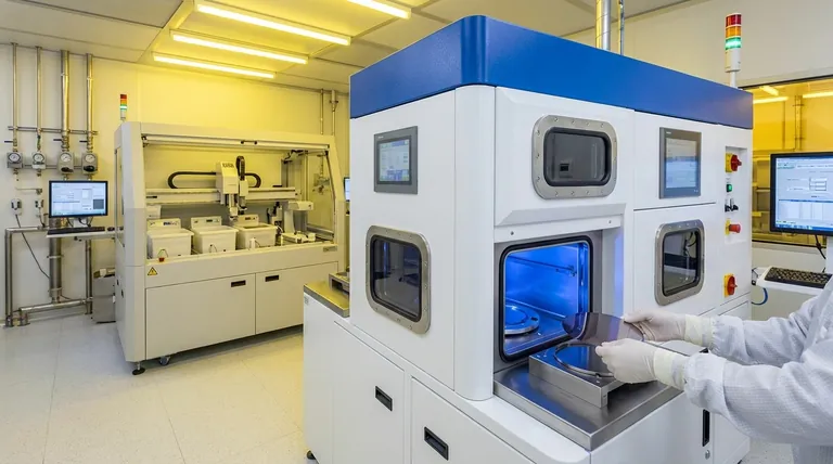
Optimize your semiconductor fabrication process with KINTEK's precision lab equipment.
Whether you are developing advanced copper interconnects or refining deposition processes, KINTEK provides the reliable PVD and ECD systems and consumables your laboratory needs. Our expertise in lab equipment ensures you achieve the uniform seed layers and void-free fills required for next-generation chips.
Contact our experts today to discuss how our solutions can enhance your manufacturing yield and performance.
Visual Guide
Related Products
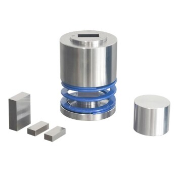
- RF PECVD System Radio Frequency Plasma-Enhanced Chemical Vapor Deposition RF PECVD
- Molybdenum Tungsten Tantalum Evaporation Boat for High Temperature Applications
- Hemispherical Bottom Tungsten Molybdenum Evaporation Boat
- Chemical Vapor Deposition CVD Equipment System Chamber Slide PECVD Tube Furnace with Liquid Gasifier PECVD Machine
- Aluminized Ceramic Evaporation Boat for Thin Film Deposition
People Also Ask
- Why is PECVD environment friendly? Understanding the Eco-Friendly Benefits of Plasma-Enhanced Coating
- Why does PECVD commonly use RF power input? For Precise Low-Temperature Thin Film Deposition
- What is an example of PECVD? RF-PECVD for High-Quality Thin Film Deposition
- What are the advantages of PECVD? Enable Low-Temperature, High-Quality Thin-Film Deposition
- What are the benefits of PECVD? Achieve Superior Low-Temperature Thin Film Deposition