In short, Chemical Vapor Deposition (CVD) offers a powerful combination of versatility, quality, and efficiency. This process is renowned for its ability to produce exceptionally pure, uniform, and durable thin films on a wide variety of materials. Its unique non-line-of-sight nature allows it to coat complex shapes evenly, a feat that many other deposition techniques cannot achieve.
The true advantage of CVD is not just its ability to apply a coating, but its power to precisely engineer material properties at the atomic level. It transforms a surface by building a new, high-performance layer from gaseous chemical precursors, enabling functionality that is otherwise impossible.
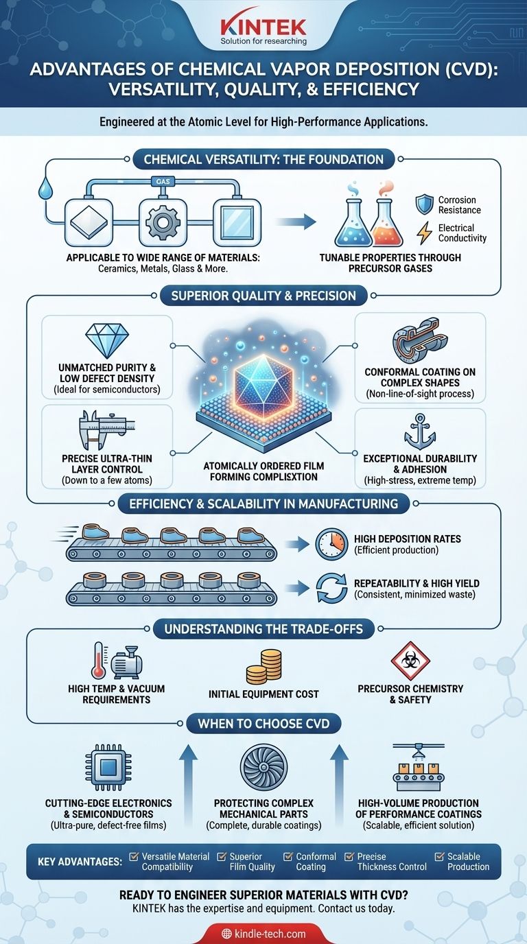
The Foundation of CVD's Power: Chemical Versatility
Chemical Vapor Deposition is defined by its use of chemical reactions, which is the source of its immense flexibility. Unlike physical methods that essentially transfer a solid material from a source to a target, CVD builds the film atom by atom from gas.
Applicable to a Wide Range of Materials
CVD is not limited to a specific class of substrate. It can be effectively used to deposit films on ceramics, metals, glass, and many other materials, making it a go-to process for diverse engineering challenges.
Tunable Properties Through Precursor Gases
The final properties of the coating are determined by the precursor gases used in the reaction. By selecting and optimizing these gases, engineers can create films designed for specific purposes, such as extreme corrosion resistance, abrasion resistance, or electrical conductivity.
Achieving Superior Film Quality and Precision
The quality of the deposited film is where CVD truly excels. The process allows for a level of control that is critical for high-performance applications.
Unmatched Purity and Low Defect Density
Because the film is constructed from highly purified gases, the resulting layer is also exceptionally pure. This is crucial for applications like semiconductors and high-performance electronics, where impurities can degrade performance. For materials like graphene, CVD is a leading method for producing large, uniform sheets with a low defect count.
Uniform, Conformal Coatings on Complex Shapes
CVD is a non-line-of-sight process. Think of it like a gas filling every corner of a room, rather than spray paint which can only hit surfaces it can see. This allows CVD to apply a perfectly uniform and conformal coating over intricate and complex geometries, ensuring complete protection and consistent properties.
Precise Control Over Ultra-Thin Layers
The process allows for meticulous control over film thickness, enabling the creation of ultra-thin layers just a few atoms thick. This precision is essential for manufacturing modern electrical circuits, optical coatings, and other micro-scale devices.
Exceptional Durability and Adhesion
The chemical bond formed between the substrate and the deposited film results in commendable adhesion. These coatings are highly durable and can withstand high-stress environments, extreme temperatures, and significant temperature variations without failing.
Understanding the Trade-offs
While powerful, CVD is not a universal solution. Understanding its operational requirements is key to making an informed decision.
High-Temperature and Vacuum Requirements
Many CVD processes require high temperatures to drive the necessary chemical reactions, which can limit the types of substrate materials that can be used. The process is also typically performed in a vacuum chamber, adding to the equipment's complexity and cost.
Precursor Chemistry and Safety
The precursor gases used in CVD can be toxic, flammable, or corrosive, requiring sophisticated handling procedures and safety protocols. The chemistry itself can be complex to develop and optimize for new materials or applications.
Initial Equipment Cost
Compared to simpler coating methods, the initial capital investment for a CVD system can be significant. The need for vacuum systems, gas handling, and temperature control makes it a more advanced manufacturing process.
Efficiency and Scalability in Manufacturing
For the right application, CVD is a highly effective and scalable manufacturing technique.
High Deposition Rates
Once optimized, CVD can achieve relatively high deposition rates compared to some other precision deposition techniques. This makes it efficient for coating parts in a production environment.
Repeatability and High Yield
The precise control over process parameters—such as temperature, pressure, and gas flow—leads to a highly repeatable outcome. This ensures consistency from batch to batch and results in a high manufacturing yield, minimizing wasted material and time.
When to Choose Chemical Vapor Deposition
Your choice of deposition technology should be guided by your end goal.
- If your primary focus is cutting-edge electronics or semiconductors: CVD is the superior choice for creating the ultra-pure, defect-free, and precisely thin films required for high-performance devices.
- If your primary focus is protecting complex mechanical parts: CVD's non-line-of-sight capability provides complete and durable coatings for wear, corrosion, and thermal protection on intricate geometries.
- If your primary focus is high-volume production of performance coatings: A well-established CVD process offers a scalable, efficient, and repeatable solution for manufacturing.
Ultimately, you should choose CVD when the performance, purity, and conformity of the film are more critical than the initial cost and complexity of the setup.
Summary Table:
| Key Advantage | Description |
|---|---|
| Versatile Material Compatibility | Deposits films on ceramics, metals, glass, and more. |
| Superior Film Quality | Creates exceptionally pure, uniform, and durable coatings. |
| Conformal Coating | Non-line-of-sight process evenly coats complex 3D shapes. |
| Precise Thickness Control | Enables the creation of ultra-thin layers, down to a few atoms. |
| Scalable Production | Offers high deposition rates and excellent batch-to-batch repeatability. |
Ready to Engineer Superior Materials with CVD?
If your laboratory demands high-purity, durable thin films for applications in semiconductors, advanced electronics, or protective coatings for complex parts, KINTEK has the expertise and equipment you need. Our CVD solutions are designed to deliver the precision and performance critical to your research and production.
Contact us today using the form below to discuss how our lab equipment can enhance your capabilities and drive your projects forward.
Visual Guide
Related Products
- Chemical Vapor Deposition CVD Equipment System Chamber Slide PECVD Tube Furnace with Liquid Gasifier PECVD Machine
- Customer Made Versatile CVD Tube Furnace Chemical Vapor Deposition Chamber System Equipment
- Microwave Plasma Chemical Vapor Deposition MPCVD Machine System Reactor for Lab and Diamond Growth
- 915MHz MPCVD Diamond Machine Microwave Plasma Chemical Vapor Deposition System Reactor
- HFCVD Machine System Equipment for Drawing Die Nano-Diamond Coating
People Also Ask
- How are carbon nanotubes grown? Master Scalable Production with Chemical Vapor Deposition
- What is plasma enhanced chemical vapor deposition PECVD equipment? A Guide to Low-Temperature Thin Film Deposition
- Why is Chemical Vapor Deposition (CVD) equipment uniquely suited for constructing hierarchical superhydrophobic structures?
- What happens during deposition chemistry? Building Thin Films from Gaseous Precursors
- How expensive is chemical vapor deposition? Understanding the True Cost of High-Performance Coating


