The primary advantages of ion beam sputtering (IBS) are its ability to produce exceptionally high-quality thin films with superior adhesion, unparalleled precision and control over the deposition process, and significant material versatility. This is achieved by using a high-energy ion beam to physically bombard a target, ejecting atoms that deposit onto a substrate with far more energy than in conventional evaporation methods, resulting in dense, uniform, and strongly bonded coatings.
Ion beam sputtering is not just another deposition technique; it is a precision engineering tool. Its core advantage lies in decoupling the ion source from the target material, allowing for independent control that produces films with a density and adhesion that lower-energy methods simply cannot replicate.
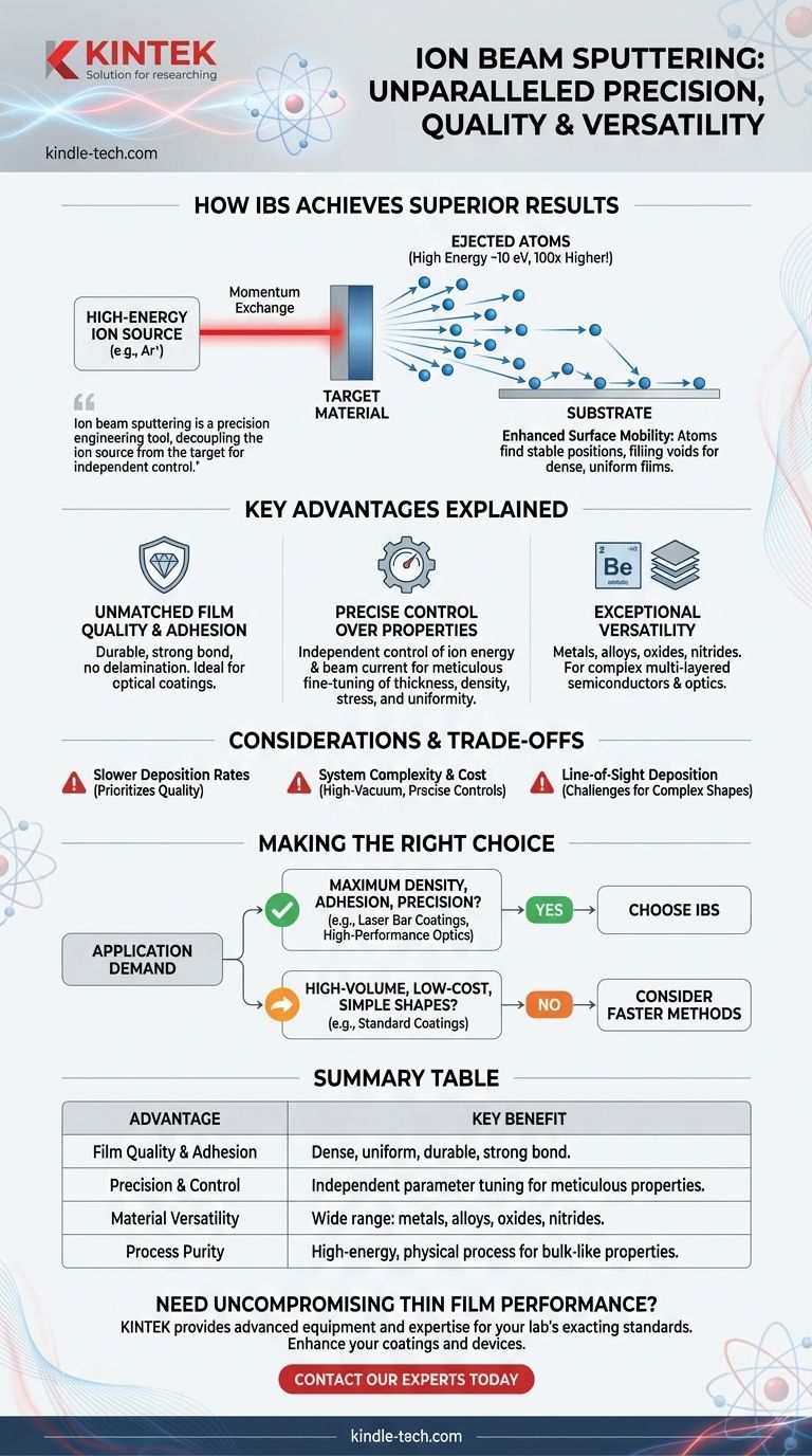
How Ion Beam Sputtering Achieves Superior Results
To understand the advantages of IBS, we must first look at its fundamental mechanism. Unlike processes that rely on heat to evaporate material, ion beam sputtering is a purely physical, high-energy process.
The Principle of Momentum Exchange
The process begins with an ion source generating a focused, high-energy beam of ions (typically an inert gas like argon). This beam is aimed at a solid "target" material. The ions strike the target with such force that they transfer their momentum to the target atoms, knocking them loose in a process known as sputtering.
High-Energy Deposition
The ejected target atoms travel toward the substrate with an average energy of around 10 eV. This is approximately 100 times higher than the energy of particles deposited through traditional vacuum evaporation.
Enhanced Surface Mobility
This high kinetic energy is the key to the quality of IBS films. When the sputtered particles arrive at the substrate, they have enough energy to move around on the surface before settling into their final position.
The Result: Densely Packed, High-Quality Films
This surface migration allows the atoms to find the most stable, low-energy positions, filling in microscopic voids. The result is a thin film that is exceptionally dense, uniform, and free of defects, with properties that often approach those of the bulk material.
The Key Advantages Explained
The unique physics of ion beam sputtering translates directly into tangible benefits for demanding applications.
Unmatched Film Quality and Adhesion
The high energy of the depositing particles creates a far stronger bond with the substrate than other methods. This exceptional adhesion ensures the film is durable and will not delaminate, which is critical for high-performance components like optical coatings.
Precise Control Over Film Properties
Because the ion source is separate from the target and substrate, engineers can independently control key parameters like ion energy, beam current, and angle of incidence. This allows for meticulous fine-tuning of film thickness, density, stress, and uniformity across the substrate.
Exceptional Versatility
Ion beam sputtering can be used with a vast range of materials, including metals, alloys, and dielectric compounds like oxides and nitrides. This makes it an indispensable technique for fabricating complex, multi-layered structures for semiconductors and precision optics.
Common Pitfalls and Trade-offs
While powerful, ion beam sputtering is a specialized technique with specific considerations that make it unsuitable for every task.
Slower Deposition Rates
The meticulous, controlled nature of IBS generally results in a slower film growth rate compared to methods like thermal evaporation or magnetron sputtering. It prioritizes quality over speed.
System Complexity and Cost
The equipment required for ion beam sputtering, particularly the high-performance ion source, is more complex and expensive than that used for simpler deposition methods. The process demands a high-vacuum environment and precise controls, adding to the operational overhead.
Line-of-Sight Deposition
Like many physical vapor deposition techniques, IBS is a line-of-sight process. The sputtered material travels in a straight line from the target to the substrate, which can make it challenging to uniformly coat complex, three-dimensional shapes without sophisticated substrate manipulation.
Making the Right Choice for Your Application
Choosing ion beam sputtering depends entirely on whether your application demands the highest possible level of performance and precision.
- If your primary focus is maximum film density, adhesion, and durability: IBS is the superior choice, especially for critical applications like laser bar coatings and high-performance optics.
- If your primary focus is precise control over thickness and uniformity: The independent control offered by IBS is essential for manufacturing complex microelectronics and semiconductor devices.
- If your primary focus is high-volume, low-cost coating on simple shapes: A faster, less complex method like thermal evaporation or magnetron sputtering may be a more practical and economical solution.
Ultimately, ion beam sputtering is the definitive choice for applications where the performance of the thin film cannot be compromised.
Summary Table:
| Advantage | Key Benefit |
|---|---|
| Film Quality & Adhesion | Produces dense, uniform films with exceptional durability and strong bonding to the substrate. |
| Precision & Control | Independent control over ion energy and beam current allows meticulous tuning of film properties. |
| Material Versatility | Capable of depositing a wide range of materials, including metals, alloys, oxides, and nitrides. |
| Process Purity | High-energy, purely physical process results in films with properties close to the bulk material. |
Need Uncompromising Thin Film Performance for Your Lab?
If your research or production demands the highest levels of film density, adhesion, and precision control, the ion beam sputtering process is the definitive solution. KINTEK specializes in providing advanced lab equipment and consumables to meet these exacting standards.
Our expertise can help you integrate this powerful technology to enhance your optical coatings, semiconductor devices, and other critical applications. Let's discuss how we can support your specific laboratory needs.
Contact our experts today to explore the right sputtering solution for you.
Visual Guide
Related Products
- Chemical Vapor Deposition CVD Equipment System Chamber Slide PECVD Tube Furnace with Liquid Gasifier PECVD Machine
- Spark Plasma Sintering Furnace SPS Furnace
- E Beam Crucibles Electron Gun Beam Crucible for Evaporation
- RF PECVD System Radio Frequency Plasma-Enhanced Chemical Vapor Deposition RF PECVD
- Electron Beam Evaporation Coating Gold Plating Tungsten Molybdenum Crucible for Evaporation
People Also Ask
- What are the advantages of chemical vapor deposition? Achieve Superior Thin Films for Your Lab
- How expensive is chemical vapor deposition? Understanding the True Cost of High-Performance Coating
- What happens during deposition chemistry? Building Thin Films from Gaseous Precursors
- What are the processes of vapor phase deposition? Understand CVD vs. PVD for Superior Thin Films
- How are carbon nanotubes grown? Master Scalable Production with Chemical Vapor Deposition


