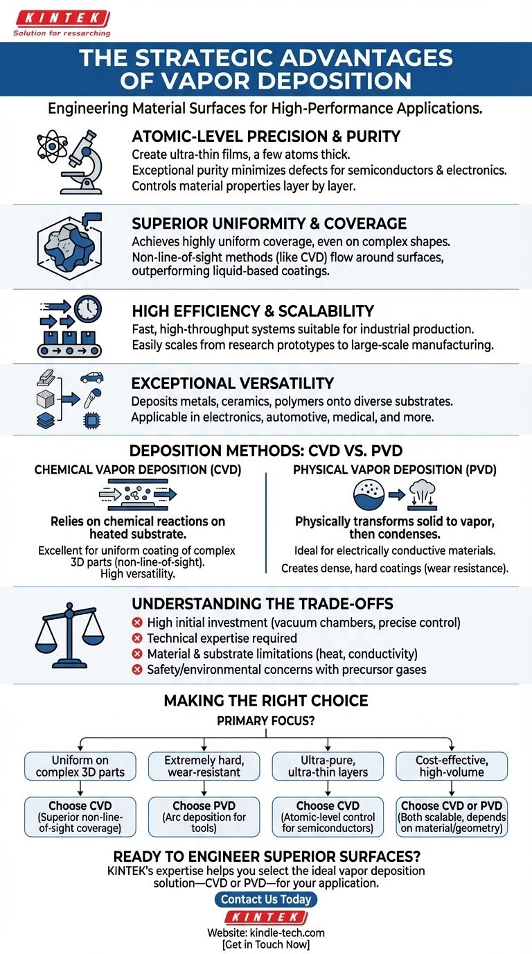
At its core, vapor deposition is a family of processes used to create exceptionally high-performance thin films and coatings. Its primary advantages are the ability to control material properties with atomic-level precision, achieve highly uniform coverage even on complex shapes, and produce coatings of extremely high purity and quality for a vast range of applications.
The true power of vapor deposition lies not just in applying a coating, but in fundamentally engineering a material's surface, layer by layer, to achieve properties that are impossible to obtain with bulk materials alone.
Why Vapor Deposition Excels: A Deeper Look
To understand the value of this technology, we must look beyond the surface and examine the specific capabilities that make it indispensable in modern manufacturing, from microchips to medical implants.
Unparalleled Precision and Purity
Vapor deposition techniques allow for the creation of ultra-thin films, sometimes just a few atoms thick. This level of control is essential in applications like manufacturing electrical circuits and semiconductors.
Because the process starts with gaseous precursors or vaporized materials in a controlled environment, the resulting films can be exceptionally pure and dense. This minimizes defects and maximizes performance.
Superior Uniformity and Coverage
A key advantage of certain methods, particularly Chemical Vapor Deposition, is their non-line-of-sight nature. This means the gaseous precursor material can flow around and coat all surfaces of a complex, three-dimensional object with a perfectly uniform layer.
This stands in stark contrast to many liquid-based or line-of-sight coating methods, which struggle to evenly coat intricate geometries, leading to inconsistencies in thickness and performance.
High Efficiency and Scalability
Modern vapor deposition systems are designed for high throughput and are remarkably fast and efficient. They can achieve high deposition rates, making them suitable for high-volume industrial production.
The processes are also highly scalable. A procedure developed in a research lab can be effectively scaled up for large-scale manufacturing, ensuring consistency from prototype to final product.
Exceptional Versatility
Vapor deposition is not limited to one type of material. It can be used to deposit metals, alloys, ceramics, and polymers onto a wide variety of underlying materials, known as substrates.
This versatility makes it applicable across countless industries, including electronics, automotive parts, medical devices, and even holographic displays.
Distinguishing Between Deposition Methods
The term "vapor deposition" covers two main families, each with unique strengths. Understanding the difference is critical to selecting the right process.
Chemical Vapor Deposition (CVD)
CVD relies on chemical reactions on the substrate's surface. A precursor gas is introduced into a chamber, which then reacts or decomposes on the heated substrate to form the desired film.
Its reliance on gas flow is what enables the excellent uniformity on complex shapes. It is also highly versatile due to the wide range of possible chemical reactions.
Physical Vapor Deposition (PVD)
PVD involves physically transforming a solid material into a vapor, transporting it, and condensing it onto the substrate. A common example is cathodic arc deposition.
PVD excels at depositing materials that are difficult to vaporize chemically, such as conductive metals. The process can also impart high kinetic energy to the vaporized ions, resulting in extremely dense and hard coatings ideal for wear resistance.
Understanding the Inherent Trade-offs
No technology is without limitations. An objective evaluation requires acknowledging the challenges associated with vapor deposition.
Process Complexity and Cost
While the principles are straightforward, the equipment—involving vacuum chambers, high temperatures, and precise gas control—can have a high initial investment cost.
Operating these systems requires significant technical expertise to manage the complex interplay of pressure, temperature, and chemical precursors.
Material and Substrate Limitations
The choice of process is often dictated by the materials involved. For instance, some PVD methods are primarily suited for electrically conductive materials.
Furthermore, the high temperatures required for some CVD processes can damage sensitive substrates, limiting their application. The availability of stable, volatile precursor chemicals for CVD can also be a constraint.
Safety and Environmental Concerns
Many precursor gases used in CVD are toxic, flammable, or corrosive, necessitating stringent safety protocols and handling procedures. The byproducts of these reactions must also be managed carefully.
Making the Right Choice for Your Application
Selecting the correct deposition strategy depends entirely on your end goal.
- If your primary focus is uniform coating on complex 3D parts: Choose Chemical Vapor Deposition (CVD) for its superior non-line-of-sight coverage.
- If your primary focus is creating an extremely hard, wear-resistant coating on a metal tool: Physical Vapor Deposition (PVD) methods like arc deposition are likely the superior choice.
- If your primary focus is producing ultra-pure, ultra-thin layers for semiconductors: CVD offers the atomic-level control required for these demanding applications.
- If your primary focus is cost-effective, high-volume production: Both methods are highly scalable, but the specific material and geometry requirements will determine the most efficient option.
Ultimately, understanding these core principles empowers you to select the precise tool needed to engineer surfaces with transformative properties.
Summary Table:
| Advantage | Key Benefit | Primary Method |
|---|---|---|
| Atomic-Level Precision | Ultra-thin, high-purity films for electronics & semiconductors | CVD & PVD |
| Superior Uniformity | Non-line-of-sight coverage of complex 3D shapes | CVD |
| Exceptional Hardness & Density | Wear-resistant coatings for tools & components | PVD |
| High Versatility | Deposits metals, ceramics, polymers on various substrates | CVD & PVD |
| Scalability & Efficiency | Suitable for high-volume industrial production | CVD & PVD |
Ready to Engineer Superior Surfaces with Vapor Deposition?
Whether you're developing advanced semiconductors, durable medical implants, or high-performance automotive components, KINTEK's expertise in lab equipment and consumables can help you select the ideal vapor deposition solution. Our team specializes in matching the right technology—be it CVD for complex geometries or PVD for extreme hardness—to your specific application.
Contact us today to discuss how our solutions can bring atomic-level precision and unmatched coating performance to your laboratory or production line. Let's transform your material surfaces together.
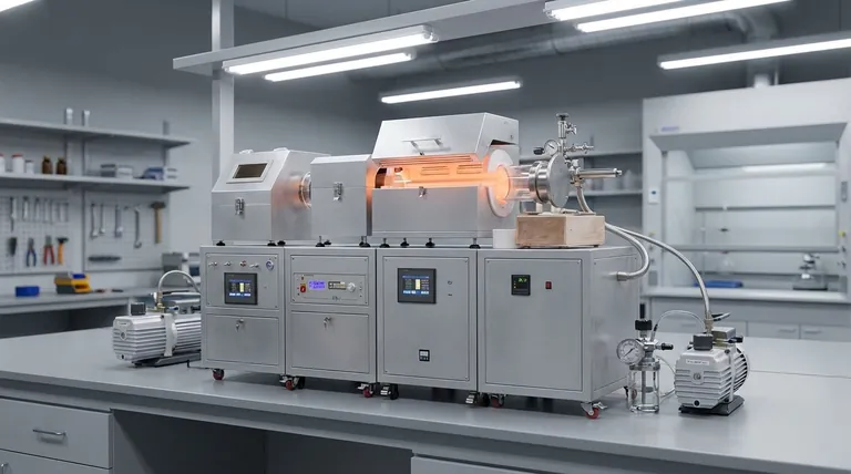
Visual Guide
Related Products
- Chemical Vapor Deposition CVD Equipment System Chamber Slide PECVD Tube Furnace with Liquid Gasifier PECVD Machine
- RF PECVD System Radio Frequency Plasma-Enhanced Chemical Vapor Deposition RF PECVD
- 915MHz MPCVD Diamond Machine Microwave Plasma Chemical Vapor Deposition System Reactor
- HFCVD Machine System Equipment for Drawing Die Nano-Diamond Coating
- Customer Made Versatile CVD Tube Furnace Chemical Vapor Deposition Chamber System Equipment
People Also Ask
- What are the core advantages of PE-CVD in OLED encapsulation? Protect Sensitive Layers with Low-Temp Film Deposition
- What types of substrates are used in CVD to facilitate graphene films? Optimize Graphene Growth with the Right Catalyst
- How expensive is chemical vapor deposition? Understanding the True Cost of High-Performance Coating
- How are carbon nanotubes grown? Master Scalable Production with Chemical Vapor Deposition
- Why is Chemical Vapor Deposition (CVD) equipment uniquely suited for constructing hierarchical superhydrophobic structures?


